 ALLPCB


In the world of printed circuit board (PCB) design, ensuring that your board can be effectively tested during manufacturing is critical. This is where Design for Testability (DFT) comes into play, particularly for In-Circuit Testing (ICT). But how do you optimize your PCB design for ICT? This handbook provides a clear answer: by following DFT guidelines, focusing on strategic PCB test point placement, adhering to ICT design rules, and prioritizing testability optimization, you can create boards that are easier and more cost-effective to test. In the detailed sections below, we'll walk you through actionable steps, practical tips, and proven strategies to achieve this goal.
Why Design for Testability Matters in PCB Manufacturing
Design for Testability, or DFT, is a set of design practices aimed at making a PCB easier to test during production. When done right, DFT reduces manufacturing costs, speeds up the testing process, and ensures higher product reliability. In-Circuit Testing (ICT) is a key method used to check for shorts, opens, and component functionality on a PCB before it moves to final assembly. Without proper DFT, ICT can become time-consuming and expensive, sometimes missing critical defects.
Statistics show that testing can account for up to 25-30% of the total production cost of a PCB. By optimizing your design for ICT, you can significantly lower these costs while improving fault detection. This handbook will guide you through the essential principles of DFT to ensure your boards are test-ready from the start.
Understanding In-Circuit Testing (ICT) and Its Challenges
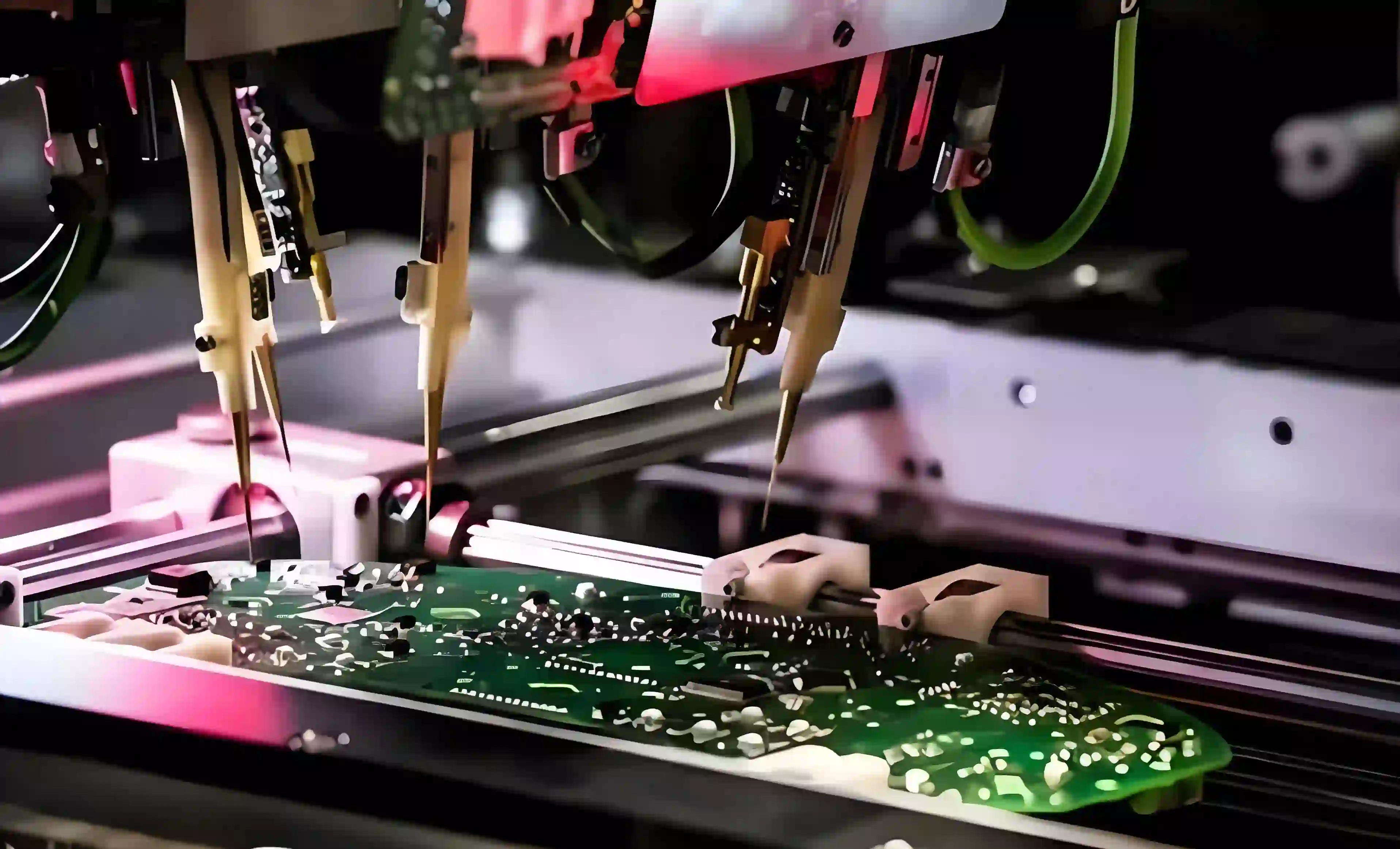
In-Circuit Testing involves using a bed-of-nails fixture or flying probe system to make electrical contact with specific points on a PCB. This method checks for issues like incorrect component placement, soldering defects, and circuit connectivity. While ICT is highly effective, it comes with challenges, especially if the PCB design isn't optimized for testing.
Common challenges include limited access to test points due to dense layouts, components blocking probe paths, and insufficient spacing for probes. These issues can lead to incomplete testing or the need for costly redesigns. By following ICT design rules, you can address these challenges early in the design phase.
Core Principles of Design for Testability (DFT)
DFT is all about planning your PCB layout with testing in mind. Below are the core principles to follow for effective testability optimization.
1. Prioritize Accessibility in Layout Design
One of the most important aspects of DFT is ensuring that test probes can easily access critical points on the board. This means placing components and traces in a way that doesn't obstruct probe contact. For instance, avoid placing tall components like capacitors or connectors near test points, as they can physically block probes.
A good rule of thumb is to maintain a clearance of at least 2.5mm (100 mils) around test points for bed-of-nails fixtures. For flying probe systems, which are often used for low-volume or prototype testing, a slightly smaller clearance of 1.5mm (60 mils) may suffice, but always check with your testing provider for specific requirements.
2. Standardize Test Point Placement
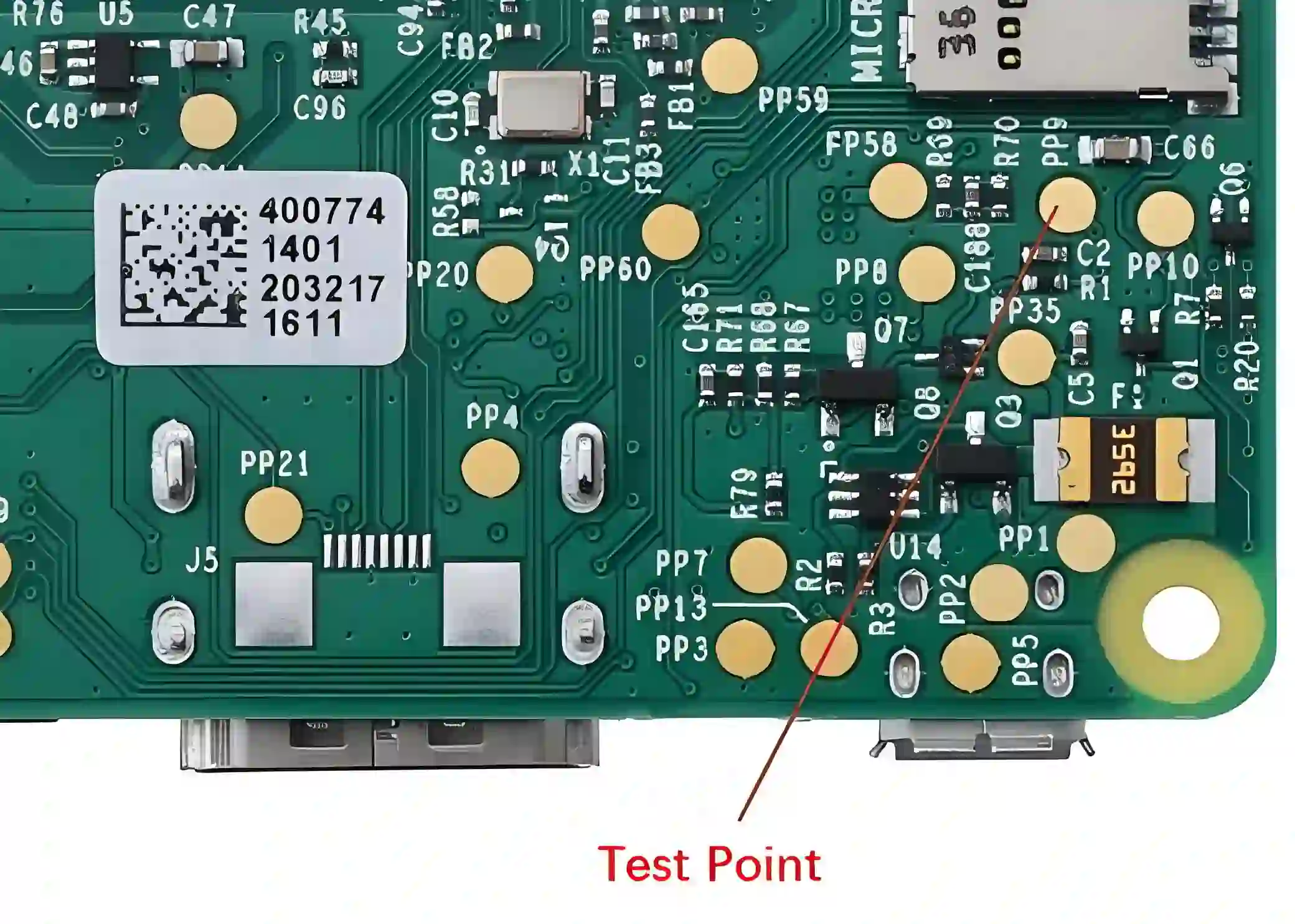
Strategic PCB test point placement is crucial for ICT. Test points are specific locations on the board where probes make contact to measure electrical signals. Place test points on every net that needs to be tested, ideally on the bottom side of the board to avoid interference with top-side components.
Ensure test points are evenly distributed and aligned in a grid pattern if possible. This makes it easier to design a bed-of-nails fixture and reduces setup time. Each test point should have a diameter of at least 1mm (40 mils) to ensure reliable probe contact. Avoid placing test points under components or near board edges where they might be damaged during handling.
3. Minimize Signal Interference
When designing for ICT, consider how test signals interact with the board's active circuits. High-speed signals, for example, can be affected by the capacitance introduced by test probes. To minimize this, avoid placing test points on high-speed nets unless absolutely necessary. If testing is required, use smaller test pads or consult with your testing team to ensure minimal interference.
For analog circuits, ensure test points are placed away from sensitive areas to prevent noise pickup. A typical guideline is to keep test points at least 5mm (200 mils) away from high-impedance nodes to avoid affecting signal integrity.
4. Optimize Component Selection for Testability
Some components are harder to test than others due to their packaging or pin configurations. For example, Ball Grid Array (BGA) components often have hidden pins that are inaccessible to ICT probes. While BGAs are sometimes unavoidable, consider adding test points on connected nets to indirectly verify their functionality.
Whenever possible, choose components with accessible pins, such as through-hole or surface-mount packages with exposed leads. This simplifies probe access and reduces the risk of missed defects during testing.
ICT Design Rules for Seamless Testing
Following specific ICT design rules ensures that your PCB is compatible with standard testing equipment and processes. Here are the key rules to implement during design.
1. Define Test Point Specifications
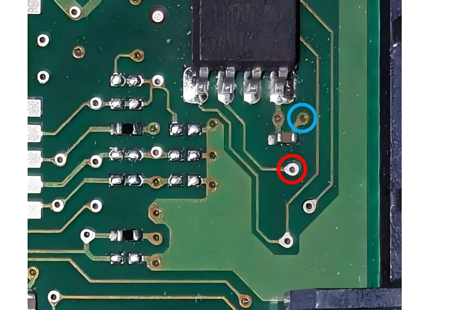
Every test point should meet certain criteria to ensure reliable contact with probes. Use pads or vias as test points, with a minimum size of 1mm (40 mils) in diameter. If using vias, ensure they are not tented (covered with solder mask) so probes can make direct contact with the copper.
Label test points clearly in your design files with identifiers like “TP1, TP2,” etc., and include a test point schedule or netlist for the testing team. This documentation saves time and prevents errors during fixture setup.
2. Ensure Proper Spacing Between Test Points
Spacing is critical for avoiding probe misalignment or interference. Maintain a minimum center-to-center distance of 2.5mm (100 mils) between test points for bed-of-nails fixtures. For flying probe systems, a slightly tighter spacing of 2mm (80 mils) may be acceptable, but always confirm with your testing provider.
Additionally, avoid clustering test points too closely in one area of the board. Distribute them evenly to prevent mechanical stress on the fixture or probes during testing.
3. Account for Board Thickness and Material
Board thickness and material can impact ICT performance. Standard ICT fixtures are designed for boards between 1.6mm and 2.0mm thick. If your board falls outside this range, inform your testing team early to ensure compatibility with their equipment.
Also, consider the dielectric constant (Dk) of your PCB material, as it affects signal propagation during testing. For high-frequency boards, using a material with a low Dk (e.g., 3.5 or below) can help maintain signal integrity during ICT.
Advanced Strategies for Testability Optimization
Beyond the basics, there are advanced techniques for testability optimization that can further streamline the ICT process and improve fault coverage.
1. Incorporate Boundary Scan Testing
For complex designs with limited physical access, boundary scan testing (JTAG) can complement ICT. Boundary scan uses built-in test logic within ICs to test connections without direct probe contact. Ensure your design includes JTAG-compliant components and dedicate test points for the JTAG signals (TCK, TMS, TDI, TDO).
While boundary scan doesn't replace ICT, it enhances coverage for hard-to-reach areas, reducing the number of physical test points needed and simplifying fixture design.
2. Simulate Testing Scenarios During Design
Modern PCB design software allows you to simulate ICT scenarios to identify potential issues before manufacturing. Use these tools to verify probe access, check for clearance violations, and ensure all critical nets have test points. Simulation can save significant time and cost by catching problems early.
3. Collaborate with Your Testing Team
Early collaboration with your testing team or manufacturing partner is invaluable. Share your design files and discuss specific ICT requirements, such as fixture type (bed-of-nails or flying probe) and test point locations. Their feedback can help refine your design for maximum testability.
Common Mistakes to Avoid in DFT for ICT
Even experienced designers can overlook key aspects of DFT. Here are common pitfalls to watch out for:
- Ignoring Test Point Accessibility: Placing test points under components or in crowded areas can render them unusable for ICT.
- Insufficient Spacing: Tight spacing between test points or components can cause probe misalignment or damage during testing.
- Lack of Documentation: Failing to provide clear test point labels or netlists can delay the testing process and lead to errors.
- Overlooking High-Speed Nets: Placing test points on sensitive high-speed lines without considering signal integrity can introduce noise or affect performance.
By keeping these mistakes in mind, you can proactively design boards that are test-ready and reliable.
Benefits of Optimizing PCB Design for ICT
Investing time in DFT guidelines and testability optimization yields significant benefits. First, it reduces testing time and costs by ensuring probes can access all necessary points without issues. Second, it improves fault detection, catching defects early in the manufacturing process. Finally, it enhances overall product reliability, leading to fewer returns and higher customer satisfaction.
For example, a well-optimized design can reduce ICT setup time by up to 20%, according to industry studies. This translates to faster production cycles and lower costs, especially for high-volume runs.
Conclusion: Building Test-Ready PCBs with DFT
Optimizing your PCB design for In-Circuit Testing is a vital step in ensuring efficient manufacturing and high-quality products. By following the Design for Testability principles outlined in this handbook—such as strategic PCB test point placement, adherence to ICT design rules, and a focus on testability optimization—you can create boards that are easier to test and more reliable in the field.
Start implementing these DFT guidelines in your next project to streamline the testing process and reduce costs. With careful planning and collaboration, you'll achieve designs that not only meet performance goals but also excel in manufacturability and quality assurance.


