 ALLPCB


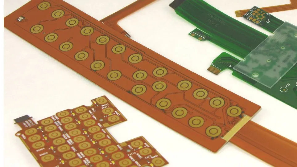
Designing and assembling flexible printed circuit boards (PCBs) can be a game-changer for modern electronics, enabling compact, lightweight, and adaptable solutions. However, achieving optimal performance requires careful attention to flexible PCB design rules, bend radius optimization, material selection for flex PCBs, minimizing stress in flex PCBAs, and high-density flex PCB design. In this guide, we'll dive deep into each of these areas, offering practical tips and actionable insights for design engineers looking to master flexible board assembly.
Whether you're working on wearables, medical devices, or aerospace applications, this comprehensive resource will help you navigate the complexities of flexible PCB design and assembly. Let's explore the key principles and techniques to ensure your projects succeed.
Understanding Flexible PCB Design Rules
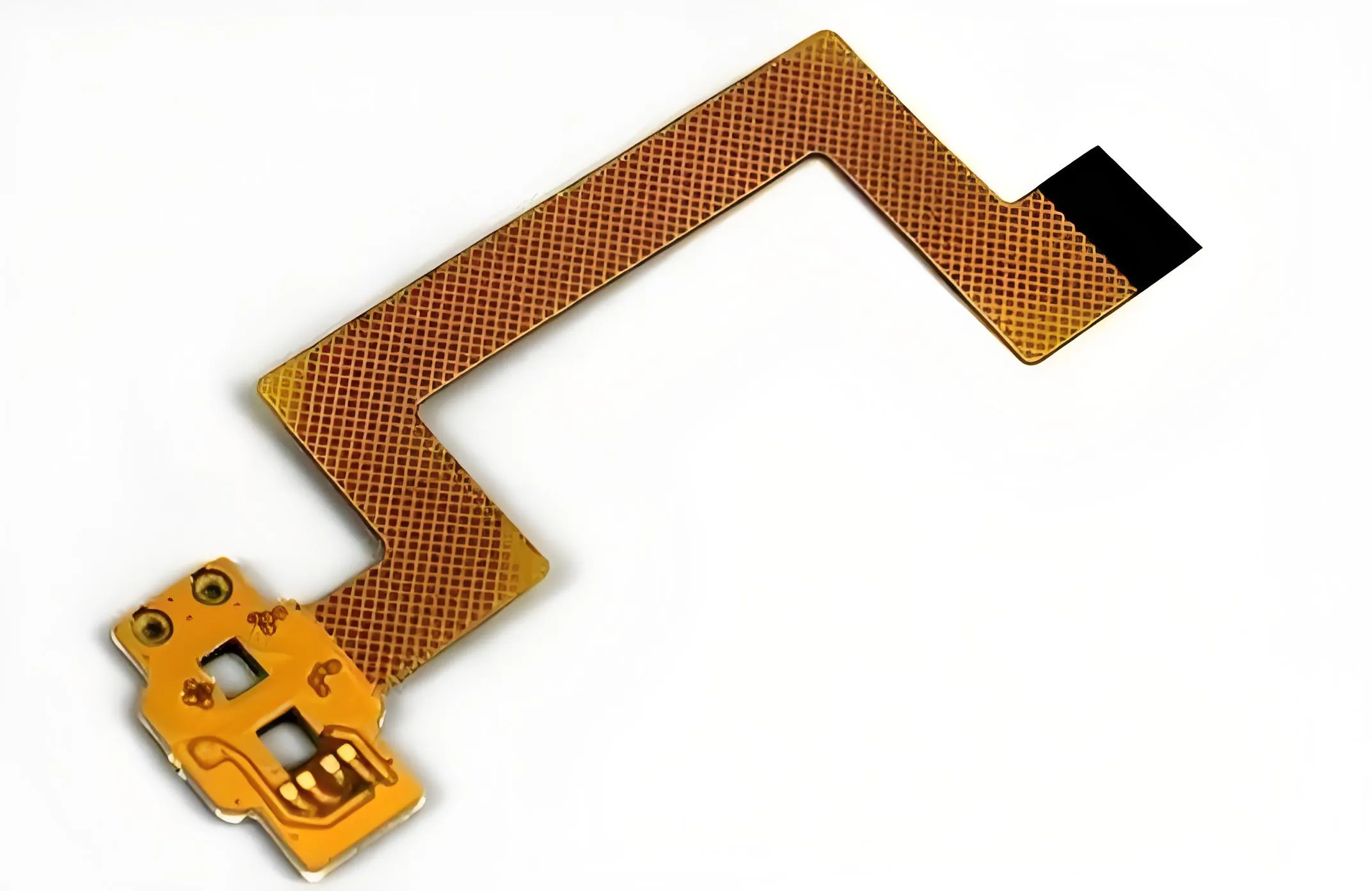
Flexible PCBs, or flex PCBs, differ significantly from rigid boards due to their ability to bend and conform to unique shapes. However, this flexibility introduces specific design challenges. Following flexible PCB design rules is essential to ensure functionality and durability.
First, consider the trace width and spacing. For high-density flex PCB design, traces should typically be kept at a minimum width of 3 mils (0.003 inches) and spacing of 3 mils to prevent signal interference and ensure manufacturability. These values can vary based on the current carrying capacity, often calculated using tools adhering to IPC-2221 standards, which suggest a current of 1 ampere per 10 mils of trace width for a 1 oz copper layer.
Another critical rule is avoiding sharp corners in trace routing. Sharp angles can create stress points during bending, leading to cracks or failures. Instead, use curved traces with a radius of at least 3 times the trace width to distribute stress evenly.
Lastly, ensure proper via design. Use teardrop-shaped vias to reinforce connections in flex areas, as they reduce the risk of pad lifting during bending. Annular rings should be larger in flex designs, ideally at least 10 mils wider than the via drill diameter, to provide extra strength.
Bend Radius Optimization: Key to Longevity
Bend radius optimization is one of the most critical aspects of flexible PCB design. The bend radius refers to the minimum radius a flex PCB can be bent without damaging the copper traces or the substrate. A poorly optimized bend radius can lead to mechanical failure or signal degradation.
As a general rule, the minimum bend radius should be at least 6 times the thickness of the flex PCB for dynamic bending applications (where the board bends repeatedly) and 3 times the thickness for static bending (a one-time bend during installation). For instance, a flex PCB with a thickness of 0.006 inches should have a minimum bend radius of 0.036 inches for dynamic applications.
To optimize the bend radius, place critical components and traces away from high-stress bend areas. Use strain relief features, such as wider traces or additional copper pours, near bend zones to distribute mechanical stress. Additionally, consider the bending direction during the design phase—flex PCBs are more durable when bent perpendicular to the trace direction rather than parallel.
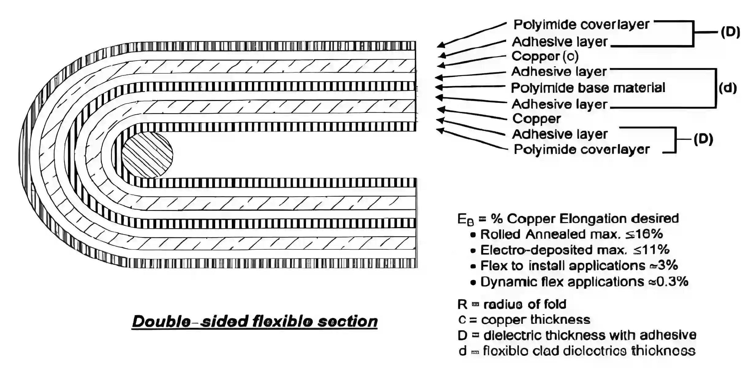
Material Selection for Flex PCBs: Finding the Right Balance
Material selection for flex PCBs plays a pivotal role in determining the board's performance, flexibility, and durability. The most common base material for flex PCBs is polyimide, known for its excellent thermal stability and flexibility. Polyimide can withstand temperatures up to 260°C, making it suitable for applications involving soldering or high operating temperatures.
For applications requiring even higher flexibility, consider thinner polyimide films (e.g., 1 mil or 25 micrometers thick) or adhesive-less laminates. Adhesive-less materials reduce the overall thickness and improve flexibility while maintaining strong copper adhesion, which is crucial for minimizing stress in flex PCBAs.
Copper foil selection is equally important. Rolled annealed (RA) copper is preferred for flex PCBs over electrodeposited (ED) copper due to its superior ductility. RA copper can endure repeated bending cycles without cracking, typically supporting up to 100,000 flex cycles in dynamic applications compared to ED copper's lower endurance of around 10,000 cycles.
Coverlay materials, which protect the copper traces, should match the base material's properties. A polyimide coverlay with a thickness of 1-2 mils offers good protection while maintaining flexibility. For high-density flex PCB design, ensure the coverlay openings are precisely aligned with pads to avoid exposure or stress points.
Minimizing Stress in Flex PCBAs: Design and Assembly Tips
Minimizing stress in flex PCBAs (printed circuit board assemblies) is crucial for ensuring reliability, especially in applications where the board undergoes frequent bending or thermal cycling. Stress can lead to trace cracking, component failure, or delamination of layers.
One effective strategy is to use stiffeners in areas where components are mounted. Stiffeners, often made of FR4 or polyimide, provide mechanical support to prevent excessive bending near sensitive components. Place stiffeners strategically, ensuring they cover at least 50% of the component area to distribute stress evenly.
During assembly, avoid placing heavy or rigid components in flex zones. For example, surface-mount components with a height greater than 0.1 inches should be mounted on rigid sections or supported by stiffeners to prevent stress concentration. Additionally, use low-stress adhesives for bonding flex layers or attaching stiffeners, as high-stress adhesives can cause delamination over time.
Thermal stress is another concern. Flex PCBs often experience thermal expansion mismatches between materials. To mitigate this, match the coefficient of thermal expansion (CTE) of the flex material with that of the components as closely as possible. Polyimide typically has a CTE of 20-30 ppm/°C, which pairs well with most surface-mount components.
High-Density Flex PCB Design: Maximizing Space and Performance
High-density flex PCB design is increasingly in demand as devices become smaller and more complex. Packing more functionality into a limited space requires careful planning to maintain signal integrity and manufacturability.
Start by optimizing the layer stack-up. A common high-density flex design might include 4-6 layers, with signal layers sandwiched between ground planes to reduce crosstalk. Keep impedance-controlled traces at a consistent width, often around 4-5 mils for 50-ohm impedance, to ensure signal integrity at speeds up to 5 Gbps or higher, depending on the dielectric constant of the material (typically 3.2-3.5 for polyimide).
Via placement is critical in high-density designs. Use microvias (diameters of 4-6 mils) instead of through-hole vias to save space and improve routing density. Stagger vias to prevent alignment issues during bending, and maintain a via-to-via spacing of at least 8 mils to avoid manufacturing defects.
Component placement also plays a big role. Group high-speed components close together to minimize trace lengths, reducing signal delay and potential interference. For example, placing a microcontroller and its associated memory chips within 0.5 inches of each other can keep trace delays under 100 picoseconds, preserving timing accuracy in high-speed circuits.
Practical Assembly Considerations for Flex PCBs
Assembly of flex PCBs requires precision to avoid damaging the delicate materials. During soldering, use a low-temperature profile to prevent thermal damage to the polyimide substrate. A peak temperature of 240°C for no more than 10 seconds is often recommended for reflow soldering of flex PCBAs.
Handling is another key factor. Flex PCBs are prone to creasing or tearing if mishandled. Use fixtures or carriers during assembly to maintain the board's shape and prevent unintended bending. Ensure that assembly personnel are trained to handle flex materials, as even a single sharp fold can compromise the board's integrity.
Finally, test the assembled flex PCBA under real-world conditions. Simulate the bending cycles and environmental stresses the board will encounter in its application. For dynamic flex applications, aim for a test cycle count of at least 10% higher than the expected lifetime (e.g., 110,000 cycles if the application requires 100,000) to ensure reliability.
Conclusion: Mastering Flexible Board Assembly
Optimizing flexible board assembly is a multifaceted challenge that demands attention to flexible PCB design rules, bend radius optimization, material selection for flex PCBs, minimizing stress in flex PCBAs, and high-density flex PCB design. By following the guidelines outlined in this comprehensive guide, design engineers can create robust, high-performing flex PCB solutions tailored to the needs of modern electronics.
From selecting the right materials like polyimide and rolled annealed copper to implementing strain relief features and precise assembly techniques, every step matters. With careful planning and execution, your flex PCB designs can achieve the perfect balance of flexibility, durability, and performance. Trust in these proven strategies to elevate your projects and deliver exceptional results in even the most demanding applications.


