 ALLPCB


If you're deciding between Laser Direct Imaging (LDI) and traditional photolithography for PCB imaging, the choice often comes down to precision, cost, and production needs. LDI offers superior accuracy and flexibility, ideal for high-density designs, while traditional photolithography remains a cost-effective option for simpler, large-scale projects. In this comprehensive guide, we'll break down the differences, advantages, and drawbacks of each method, helping you pick the best approach for your PCB manufacturing process. We'll cover LDI PCB advantages, photolithography PCB disadvantages, and provide a detailed PCB imaging comparison to ensure you have all the information you need.
What Is PCB Imaging and Why Does It Matter?
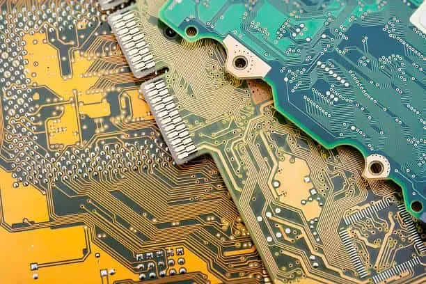
PCB imaging is a critical step in the manufacturing of printed circuit boards. It involves transferring the circuit design onto the board's surface, creating a pattern that guides the etching process to form conductive traces. The quality of imaging directly impacts the board's performance, affecting signal integrity, impedance control, and overall reliability. Whether you're working on a simple single-layer board or a complex multi-layer design with fine-pitch components, choosing the right imaging method is essential for meeting design specifications and production goals.
Understanding Laser Direct Imaging (LDI) in PCB Manufacturing
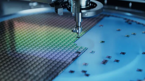
Laser Direct Imaging, or LDI, is an advanced technology that uses a computer-controlled laser beam to directly expose circuit patterns onto a photosensitive layer on the PCB substrate. Unlike traditional methods, LDI doesn't require a physical photomask. Instead, the laser draws the design with pinpoint accuracy, achieving resolutions as fine as 10 microns for line widths and spacing.
This method is particularly suited for high-density interconnect HDI PCBs, where tiny features and tight tolerances are common. LDI systems can handle complex designs with ease, supporting multi-layer boards used in smartphones, medical devices, and automotive electronics. The process is fully digital, allowing for quick design adjustments without the need for physical tools or masks.
Key LDI PCB Advantages
- High Precision: LDI achieves sub-micron accuracy, making it perfect for fine-pitch components and microvias. For example, it can consistently produce traces with widths below 25 microns, which is often necessary for modern compact devices.
- No Photomask Needed: By eliminating the need for a physical mask, LDI reduces production lead times and avoids errors caused by mask misalignment or defects.
- Flexibility: Design changes can be implemented instantly through software updates, ideal for prototyping or small-batch production runs.
- Improved Registration: LDI offers better layer-to-layer alignment in multi-layer boards, reducing signal interference and ensuring impedance values stay within tight tolerances (e.g., ±10% of target impedance like 50 ohms for high-speed signals).
- Reduced Waste: The digital nature of LDI minimizes material waste associated with mask production and rework due to imaging errors.
Challenges of LDI in PCB Imaging
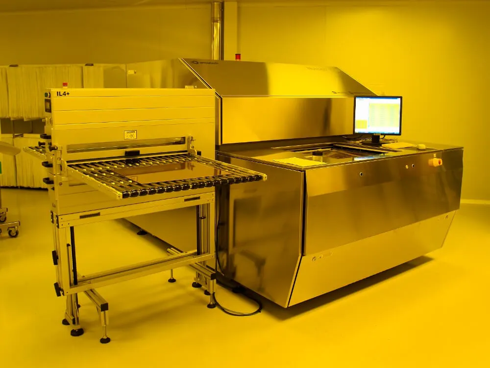
While LDI offers numerous benefits, it’s not without its downsides. The primary challenge is the initial investment. LDI equipment can cost significantly more than traditional imaging setups, often ranging from hundreds of thousands to over a million dollars for high-end systems. This makes it less accessible for smaller manufacturers or those with low-volume production needs.
Additionally, LDI can be slower for very large production runs. The laser scanning process, while precise, takes longer per board compared to exposing an entire panel at once with a photomask. For high-volume projects without complex designs, this can impact overall throughput.
Exploring Traditional Photolithography for PCB Imaging
Traditional photolithography has been the standard in PCB manufacturing for decades. This process uses a photomask—a film or glass plate with the circuit pattern printed on it—to transfer the design onto a photosensitive layer on the PCB through exposure to UV light. After exposure, the board undergoes development and etching to create the conductive traces.
This method is well-established and widely used, especially for simpler designs or high-volume production where cost efficiency is a priority. It’s a proven technology that many manufacturers are familiar with, requiring less specialized training compared to newer methods like LDI.
Benefits of Traditional Photolithography
- Cost-Effective for Large Runs: Once the photomask is created, it can be reused for thousands of boards, making photolithography economical for mass production.
- Faster for Simple Designs: Exposing an entire panel at once with UV light is quicker than scanning with a laser, especially for basic single- or double-layer boards.
- Lower Equipment Costs: The machinery for photolithography is generally less expensive than LDI systems, with basic setups costing tens of thousands of dollars rather than hundreds of thousands.
Photolithography PCB Disadvantages
Despite its affordability, traditional photolithography has limitations that can affect its suitability for modern PCB designs. These drawbacks are especially evident when dealing with high-density or intricate layouts.
- Limited Precision: Photolithography struggles with fine features, often unable to reliably produce traces narrower than 50 microns. This makes it unsuitable for HDI boards or designs with tight spacing.
- Photomask Dependency: Creating and maintaining photomasks adds time and cost to the process. Each design change requires a new mask, which can take days to produce and cost hundreds to thousands of dollars.
- Alignment Issues: Misalignment during exposure can lead to registration errors, especially in multi-layer boards, causing signal integrity issues or impedance mismatches (e.g., deviating from a target of 50 ohms by more than ±15%).
- Higher Defect Rates: Dust or scratches on the photomask can transfer defects to the board, requiring rework and increasing waste.
PCB Imaging Comparison: LDI vs. Photolithography
To help you make an informed decision, let’s compare these two methods across key factors like precision, cost, speed, and suitability for different production needs. This PCB imaging comparison will highlight where each technology shines and where it falls short.
| Criteria | Laser Direct Imaging (LDI) | Traditional Photolithography |
|---|---|---|
| Precision | High (line widths down to 10 microns) | Moderate (line widths typically above 50 microns) |
| Cost | High initial investment; lower per-unit cost for complex designs | Lower equipment cost; economical for large runs |
| Speed | Slower for large volumes due to scanning process | Faster for large panels and simple designs |
| Flexibility | Highly flexible; easy to update designs digitally | Less flexible; requires new photomask for changes |
| Suitability | Ideal for HDI, multi-layer, and small-batch production | Best for simple designs and high-volume runs |
Laser Imaging Benefits for Modern PCB Needs
The rise of compact, high-performance electronics has increased the demand for precise manufacturing techniques. Laser imaging benefits include the ability to meet these demands with unmatched accuracy and adaptability. For instance, LDI can achieve consistent impedance control for high-speed signals, ensuring values like 50 ohms or 100 ohms are maintained within ±5%—a critical factor for applications like 5G devices or high-frequency RF circuits.
Moreover, LDI supports the trend toward miniaturization. As devices shrink, components are placed closer together, requiring finer traces and smaller vias. LDI can produce microvias with diameters as small as 50 microns, enabling denser routing without sacrificing reliability. This capability is invaluable for industries pushing the boundaries of technology, from wearable tech to aerospace systems.
Direct Imaging PCB Cost: Is LDI Worth the Investment?
When evaluating direct imaging PCB cost, it’s important to consider both upfront expenses and long-term savings. LDI systems require a significant initial investment, often in the range of $500,000 to $1,500,000 for industrial-grade equipment. In contrast, a basic photolithography setup might cost $50,000 to $200,000. However, LDI can reduce costs over time by eliminating photomask expenses, which can range from $500 to $5,000 per mask depending on complexity.
For small to medium production runs or projects requiring frequent design iterations, LDI often proves more cost-effective. The ability to skip mask production saves both money and time, especially during prototyping phases. On the other hand, for high-volume manufacturing of simpler boards, traditional photolithography may still offer a better return on investment due to its lower equipment costs and faster processing speeds.
How to Choose the Right Imaging Method for Your PCB Project
Selecting between LDI and traditional photolithography depends on your specific project requirements. Here are some factors to consider:
- Design Complexity: If your PCB involves HDI, fine-pitch components, or multi-layer structures, LDI is the better choice due to its precision and registration accuracy.
- Production Volume: For large-scale production of basic designs, photolithography’s speed and lower cost per unit make it more practical.
- Budget Constraints: If upfront costs are a concern, starting with photolithography might be feasible, though consider long-term savings with LDI for complex or iterative projects.
- Time-to-Market: LDI’s flexibility for quick design changes can accelerate development cycles, which is crucial for competitive industries.
Ultimately, weigh these factors against your project goals. For cutting-edge applications demanding tight tolerances (e.g., signal speeds exceeding 10 Gbps), investing in LDI could be a game-changer. For standard applications with less stringent requirements, traditional methods might suffice.
Future Trends in PCB Imaging Technology
As the electronics industry evolves, so does PCB imaging technology. LDI is expected to become more accessible as equipment costs gradually decrease and adoption increases. Market insights suggest the LDI market could grow at a compound annual growth rate (CAGR) of over 12% through the next decade, driven by demand for HDI and flexible PCBs.
Meanwhile, advancements in photolithography, such as improved mask materials and UV light sources, aim to address some of its precision limitations. However, for most high-tech applications, LDI is likely to remain the preferred choice due to its adaptability and superior performance with modern designs.
Conclusion: Making an Informed Decision for PCB Imaging
Choosing between Laser Direct Imaging and traditional photolithography for PCB manufacturing boils down to balancing precision, cost, and production scale. LDI stands out with its LDI PCB advantages, offering unmatched accuracy and flexibility for complex, high-density designs. However, its higher initial cost may deter smaller operations. Traditional photolithography, despite its photolithography PCB disadvantages like limited precision, remains a viable, budget-friendly option for simpler, high-volume projects.
By understanding the strengths and weaknesses of each method through this PCB imaging comparison, you can align your choice with your project’s specific needs. Whether you prioritize the laser imaging benefits of LDI or aim to manage direct imaging PCB cost with photolithography, making an informed decision ensures better outcomes for your PCB production. Trust in a manufacturing partner that understands these technologies to help guide you toward success in your next project.


