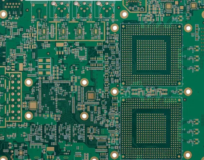
As electronic devices become increasingly complex and compact, ensuring the reliability and functionality of printed circuit boards is more critical than ever. A single defective PCB can lead to system-wide failures, product recalls, and costly repairs. That's why PCB testing is a fundamental part of the manufacturing process. Among the most widely used PCB testing methods are In-Circuit Testing, Flying Probe Testing, and Functional Testing. This article explores the principles, capabilities, advantages, and limitations of each.
Why PCB Testing Matters
Before diving into the testing methods, it's important to understand what PCB testing is designed to verify:
- Electrical connectivity of nets and traces
- Component presence, orientation, and value
- Shorts, opens, and misalignments
- Solder joint integrity
- Functional performance under real-world conditions
Testing ensures that each assembled PCB meets the electrical and functional requirements before being integrated into a final product.
In-Circuit Testing (ICT)
What is ICT?
In-Circuit Testing is an automated method used to electrically test the components and circuit paths on a populated PCB. ICT machines use a bed-of-nails fixture to access individual test points via spring-loaded pogo pins.
Key Features:
- Tests each component individually (resistors, capacitors, ICs, etc.)
- Verifies shorts, opens, incorrect components, and solder defects
- Requires dedicated test fixtures and test programs
- Typically used in high-volume production
How it Works:
The test fixture aligns with the PCB and presses down to make contact with exposed test points or vias. The tester then applies a series of electrical signals to check each component's behavior in isolation from the rest of the circuit.
Pros:
- Fast testing (seconds per board)
- High fault coverage
- Ideal for mass production
- Can detect subtle component failures (e.g., wrong resistor value)
Cons:
- Expensive to build fixtures (costs can be $5,000–$20,000 per board)
- Requires space for test points on the PCB
- Not ideal for low-volume or prototype testing
Related Reading: ICT Test Fixtures: A Deep Dive into Different Types and Their Applications
Flying Probe Testing (FPT)
What is Flying Probe Testing?
Flying Probe Testing is a fixtureless method that uses robotically controlled probes to move across the PCB and test each node sequentially. It’s ideal for low-to-medium volume production, prototypes, and boards without dedicated test points.
Key Features:
- No fixture required (uses moving probes)
- Lower upfront cost
- Slower test time compared to ICT
- Can access pads, vias, and component leads
How it Works:
The flying probes are guided by a programmed script that defines probe positions, test sequences, and electrical measurements. They contact different points on the PCB and perform continuity, insulation, and component value checks.
Pros:
- Lower cost for small production runs
- Rapid setup and programming
- Good for design validation and prototyping
- Detects shorts, opens, missing/incorrect components
Cons:
- Slower test cycle (~1–3 minutes per board)
- Less suited for very large volumes
- Limited access to high-density BGAs or hidden pins
Functional Testing (FCT)
What is Functional Testing?
Functional Testing verifies that a fully assembled PCB behaves as intended in a real-world operating environment. It's often done after ICT or Flying Probe, using custom test setups that simulate final use conditions.
Key Features:
- Simulates actual application scenarios
- May include power-on tests, communication interface checks, sensor readings, etc.
- Requires custom test jigs and software
- Ensures end-user functionality
How it Works:
The PCB is powered and connected to a test fixture that mimics its final environment. The tester may send signals via USB, Ethernet, I²C, SPI, etc., and monitor outputs to validate performance. Some setups include thermal chambers or vibration tables for environmental testing.
Pros:
- Confirms the entire system’s functionality
- Identifies complex, systemic, or intermittent faults
- Essential for critical or safety-related products
Cons:
- Slower and more complex
- Requires customized hardware/software
- Higher cost per test
Comparing the Three Methods
Related Reading: Flying Probe vs. Fixture Testing: Cost Comparison
Best Practices in PCB Testing
To ensure effective testing, follow these recommendations:
- Design for Testability (DFT): Add test pads, breakouts, and software access points during the design stage.
- Combine test methods: For high reliability, combine ICT/FPT with functional testing.
- Use test point optimization: Minimize test fixture cost by optimizing test point layout.
- Automate where possible: For large volumes, invest in automated test equipment (ATE) and data logging.
- Validate firmware: Ensure functional tests include checks for correct firmware upload and MCU/FPGA operation.
Conclusion
Testing is not an afterthought—it is a mission-critical part of PCB production. Choosing the right method depends on your project's volume, complexity, and reliability requirements. In-Circuit Testing offers speed and coverage for large-scale production. Flying Probe Testing is ideal for prototyping and flexible volumes. Functional Testing ensures that the final product meets performance expectations in real-world applications.
By understanding and integrating these testing methodologies into your production workflow, you can greatly reduce failure rates, lower returns, and improve customer satisfaction.
 ALLPCB


