 ALLPCB


If you're new to electronics design and wondering how to create an FR-4 PCB prototype, you're in the right place. FR-4 PCB prototyping is the process of designing and building a test version of a printed circuit board using FR-4 material, a popular and cost-effective choice for many applications. In this guide, we'll walk you through the entire FR-4 PCB prototyping process step by step, from design to assembly, ensuring you have the knowledge to bring your ideas to life.
Whether you're working on a hobby project or developing a product for market, understanding the FR-4 PCB prototype manufacturing process is key to success. Let’s dive into the details of FR-4 PCB prototype design, manufacturing, assembly, and more, tailored for beginners with actionable tips and clear explanations.
What is FR-4 and Why Use It for PCB Prototyping?
FR-4 is a type of material used in printed circuit boards (PCBs). It stands for "Flame Retardant 4" and is made of woven fiberglass cloth with an epoxy resin binder. This combination makes FR-4 strong, lightweight, and resistant to heat and moisture, which is why it’s the go-to choice for most PCB projects.
For beginners, FR-4 is ideal because it’s affordable and widely available. It supports a variety of applications, from simple single-layer boards to more complex multi-layer designs. Its dielectric constant, typically around 4.5, ensures stable electrical performance, making it suitable for frequencies up to several gigahertz. Additionally, FR-4 can handle temperatures up to 130°C without degrading, which is more than enough for most consumer electronics.
Benefits of FR-4 PCB Prototyping
Prototyping with FR-4 material offers several advantages:
- Cost-Effective: FR-4 is one of the most budget-friendly materials for PCB prototyping, making it accessible for beginners and small-scale projects.
- Durability: Its mechanical strength and resistance to environmental factors ensure your prototype can withstand testing conditions.
- Versatility: FR-4 supports a wide range of designs, from low-frequency circuits to moderately high-speed applications.
- Availability: Most PCB prototyping services offer FR-4 as a standard material, ensuring quick turnaround times.
With these benefits in mind, let’s explore the step-by-step FR-4 PCB prototyping process to help you create a functional prototype.
Step-by-Step Guide to FR-4 PCB Prototyping Process
The FR-4 PCB prototyping process involves several stages, each critical to ensuring your board works as intended. Below, we break it down into manageable steps for beginners.
Step 1: Define Your Project Requirements
Before diving into design, take time to outline what your PCB needs to do. Consider the following:
- What is the purpose of your circuit? Is it for a simple LED project or a complex microcontroller system?
- How many layers will your PCB need? Most beginners start with single or double-layer boards using FR-4, which are easier to design and cheaper to produce.
- What are the size constraints? Measure the space where your PCB will fit to determine board dimensions.
- What are the electrical requirements? For example, ensure the FR-4 material can handle your circuit’s voltage and current needs—typically up to 100V and several amps for standard designs.
Having a clear plan reduces errors during the FR-4 PCB prototype design phase and saves time later.
Step 2: Create a Schematic for FR-4 PCB Prototype Design
The next step in the FR-4 PCB prototyping process is designing a schematic—a blueprint of how components connect electrically. Use design software to draw your circuit. Popular tools are widely available and often free for basic use.
In your schematic, include all components like resistors, capacitors, and ICs, and define their connections. Double-check values and connections to avoid mistakes. For instance, ensure a resistor’s value matches your calculations—say, 220 ohms for an LED circuit with a 5V supply to limit current to around 20mA.
Step 3: Design the PCB Layout
Once your schematic is ready, convert it into a physical layout. This involves placing components on a virtual board and routing traces (conductive paths) between them. Keep these tips in mind for FR-4 PCB prototype design:
- Place components logically—group related parts together to minimize trace lengths.
- Ensure traces are wide enough for the current they’ll carry. For example, a trace width of 0.254mm (10 mils) is often sufficient for low-current signals, but high-current paths may need 1mm or more.
- Avoid crossing traces on the same layer to prevent interference. Use vias (small holes) to route traces to another layer if needed.
- Leave enough clearance between traces—typically 0.2mm or more—to prevent short circuits.
FR-4’s properties, like its dielectric constant of 4.5, help maintain signal integrity during layout, especially for beginners working on low to medium-speed circuits.
Step 4: Generate Gerber Files for Manufacturing
After finalizing your layout, export it as Gerber files—a standard format used in FR-4 PCB prototype manufacturing. These files include layers for copper traces, solder mask, silkscreen, and drill holes. Most design tools have built-in options to generate these files.
Check your Gerber files using a viewer tool to ensure there are no errors, such as missing traces or misaligned layers. This step is crucial before sending your design to a manufacturer for FR-4 PCB prototyping services.
Step 5: Choose FR-4 PCB Prototyping Services
Selecting a reliable provider for FR-4 PCB prototyping services is vital. Look for a service that offers:
- Quick turnaround times—often 4-5 days for small batches of prototypes.
- Support for FR-4 material with standard specifications like 1.6mm thickness and 1oz copper weight.
- Options for small quantities, such as 5-10 pieces, to keep costs low during testing.
Submit your Gerber files along with specifications like board thickness and layer count. Many services provide instant quotes based on these details, making budgeting easier for beginners.
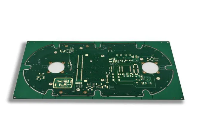
Step 6: FR-4 PCB Prototype Manufacturing Process
Once your files are with the manufacturer, the FR-4 PCB prototype manufacturing process begins. Here’s a simplified overview of what happens:
- Material Preparation: A sheet of FR-4 material, typically 1.6mm thick, is cut to size.
- Copper Etching: Copper layers are etched to create traces based on your design. Standard copper thickness is 1oz per square foot (about 35 micrometers).
- Drilling: Holes for vias and component leads are drilled with precision, often as small as 0.3mm in diameter.
- Solder Mask Application: A protective green layer (solder mask) is applied to prevent short circuits and oxidation.
- Silkscreen: Labels and markings are printed for component placement.
- Testing: Basic electrical tests ensure there are no open or short circuits before shipping.
This process ensures your FR-4 PCB prototype matches your design and is ready for assembly.
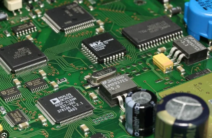
Step 7: FR-4 PCB Prototype Assembly
With your bare FR-4 PCB in hand, it’s time for assembly—placing and soldering components onto the board. For beginners, manual assembly is common for small projects. Follow these steps:
- Place components according to the silkscreen markings. Start with smaller parts like resistors and capacitors before larger ones like connectors.
- Use a soldering iron (around 300°C for leaded solder) to attach components. Apply solder to pads, not the iron tip, for clean joints.
- Inspect for cold solder joints—dull or cracked connections that can fail under stress.
For larger or complex designs, consider professional FR-4 PCB prototype assembly services. These use automated pick-and-place machines for accuracy and speed, especially for surface-mount components with pitches as small as 0.5mm.
Step 8: Testing Your FR-4 PCB Prototype
Testing is a critical part of the FR-4 PCB prototyping process. Power up your board and check for functionality. Use a multimeter to verify voltages at key points—for instance, ensure a 5V regulator outputs close to 5V, within a tolerance of ±0.1V.
- Check for shorts or open circuits if the board doesn’t work.
- Test signal integrity for high-speed designs, ensuring minimal noise or crosstalk on FR-4, which supports speeds up to a few gigahertz.
- Iterate on your design if issues arise, making adjustments and ordering a revised prototype.
Common Challenges in FR-4 PCB Prototyping and How to Avoid Them
Beginners often face hurdles during FR-4 PCB prototype manufacturing and assembly. Here are some common issues and solutions:
- Design Errors: Missing connections or incorrect footprints can ruin a prototype. Always double-check your schematic and layout against datasheets.
- Signal Interference: Poor trace routing can cause noise. Keep high-speed traces short and away from power lines on your FR-4 board.
- Overheating During Soldering: Excessive heat can damage FR-4 or components. Use a temperature-controlled iron and work quickly.
- Manufacturing Delays: Incomplete or incorrect Gerber files can delay production. Verify files before submission to FR-4 PCB prototyping services.
Tips for Successful FR-4 PCB Prototyping
To make your FR-4 PCB prototyping journey smoother, keep these tips in mind:
- Start with simple designs to build confidence before tackling complex multi-layer boards.
- Use design rule checks (DRC) in your software to catch spacing or clearance errors early.
- Order a few extra prototypes (e.g., 5 instead of 2) to account for testing failures.
- Document every step—schematics, layouts, and test results—to streamline future iterations.
Conclusion: Start Your FR-4 PCB Prototyping Journey Today
FR-4 PCB prototyping is an exciting and accessible way to bring your electronic ideas to life. By following this step-by-step guide, you’ve learned the essentials of the FR-4 PCB prototyping process, from design and manufacturing to assembly and testing. With FR-4’s affordability, durability, and versatility, it’s the perfect material for beginners to experiment and innovate.
Whether you’re creating a small hobby project or laying the groundwork for a larger product, mastering FR-4 PCB prototype design and manufacturing opens up endless possibilities. Take the first step by defining your project requirements and exploring reliable FR-4 PCB prototyping services to turn your vision into reality.


