ALLPCB


In the fast-paced world of electronics design, 3D printing PCBs is transforming how engineers prototype and manufacture custom circuit boards. This innovative technology, also known as additive manufacturing, offers speed, flexibility, and cost-efficiency compared to traditional methods. Whether you're exploring 3D printed PCB materials, curious about the additive manufacturing PCB process, or looking into multilayer PCB 3D printing, this guide will dive deep into how 3D printing is reshaping the industry. We'll also cover conductive ink PCB printing and break down 3D PCB prototyping cost to help you make informed decisions.
At its core, 3D printing for PCBs allows designers to create complex, customized boards layer by layer, reducing lead times and enabling rapid iteration. In this blog, we'll explore the technology behind it, the materials used, the benefits for prototyping, and what you need to know to get started.
What Is 3D Printing for PCBs and Why Does It Matter?
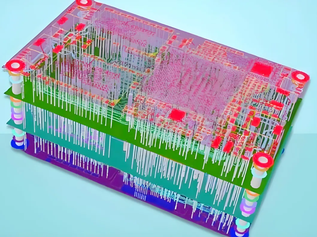
3D printing for PCBs refers to the process of creating printed circuit boards using additive manufacturing techniques. Unlike traditional subtractive methods—where material is removed from a solid board to form circuits—3D printing builds the board layer by layer, adding only the necessary materials. This approach minimizes waste and allows for intricate designs that were once impossible or too costly to produce.
The significance of this technology lies in its ability to accelerate prototyping and custom manufacturing. Engineers can test designs within hours instead of waiting weeks for fabricated boards. Additionally, 3D printing supports the creation of non-planar or flexible circuits, opening doors to innovative applications in wearables, aerospace, and medical devices.
How 3D Printing Differs from Traditional PCB Manufacturing
Traditional PCB manufacturing involves etching copper layers on a substrate, often requiring multiple steps like drilling, plating, and masking. These processes are time-consuming and generate significant material waste. In contrast, the additive manufacturing PCB process deposits conductive and insulating materials only where needed, streamlining production and reducing environmental impact.
The Additive Manufacturing PCB Process: How It Works
The additive manufacturing PCB process involves several key steps, each designed to build a functional circuit board with precision. Here's a breakdown of how it typically works:
- Design Creation: Engineers use CAD software to design the PCB layout, specifying conductive traces, insulating layers, and component placements. The design is then converted into a format compatible with 3D printing systems.
- Material Deposition: A 3D printer deposits insulating substrate materials (like polymers) and conductive materials (like silver-based inks) layer by layer. This can be done using techniques such as inkjet printing or extrusion.
- Curing or Sintering: After deposition, the conductive materials are often cured or sintered to enhance conductivity. For instance, some systems use heat or UV light to solidify the ink, achieving impedance values as low as 0.1 ohms per square for certain silver inks.
- Finishing: Additional layers or components may be added manually or via automated pick-and-place systems. The final board is tested for electrical performance, ensuring signal speeds meet design specs (e.g., supporting frequencies up to 1 GHz for high-speed applications).
This process allows for rapid iterations, as changes to the design can be implemented and printed within hours. It’s especially useful for prototyping, where speed and adaptability are critical.
Exploring 3D Printed PCB Materials
The choice of 3D printed PCB materials plays a crucial role in the performance and durability of the final board. These materials generally fall into two categories: substrates and conductive elements.
Substrate Materials
Substrates form the insulating base of the PCB. Common materials used in 3D printing include:
- Polymers: Materials like PLA or PET are often used for their flexibility and ease of printing. They’re ideal for prototyping but may not withstand high temperatures (typically limited to under 80°C).
- Composites: Advanced composites with fiberglass or ceramic fillers offer better thermal stability (up to 150°C) and mechanical strength, suitable for more demanding applications.
- Flexible Materials: Polyimide-based materials enable the creation of flexible PCBs, perfect for wearable electronics.
Conductive Materials
For the conductive traces, conductive ink PCB printing is a game-changer. These inks are typically made of:
- Silver Nanoparticles: Widely used due to their high conductivity (around 10^6 S/m), though they can be expensive.
- Copper-Based Inks: A more cost-effective alternative, though they require careful handling to prevent oxidation. Conductivity is slightly lower, often around 10^5 S/m.
- Graphene Inks: Emerging as a lightweight, highly conductive option with excellent flexibility, ideal for innovative designs.
Choosing the right materials depends on the application. For high-frequency circuits, low-loss substrates and high-conductivity inks are essential to maintain signal integrity at speeds exceeding 500 MHz.
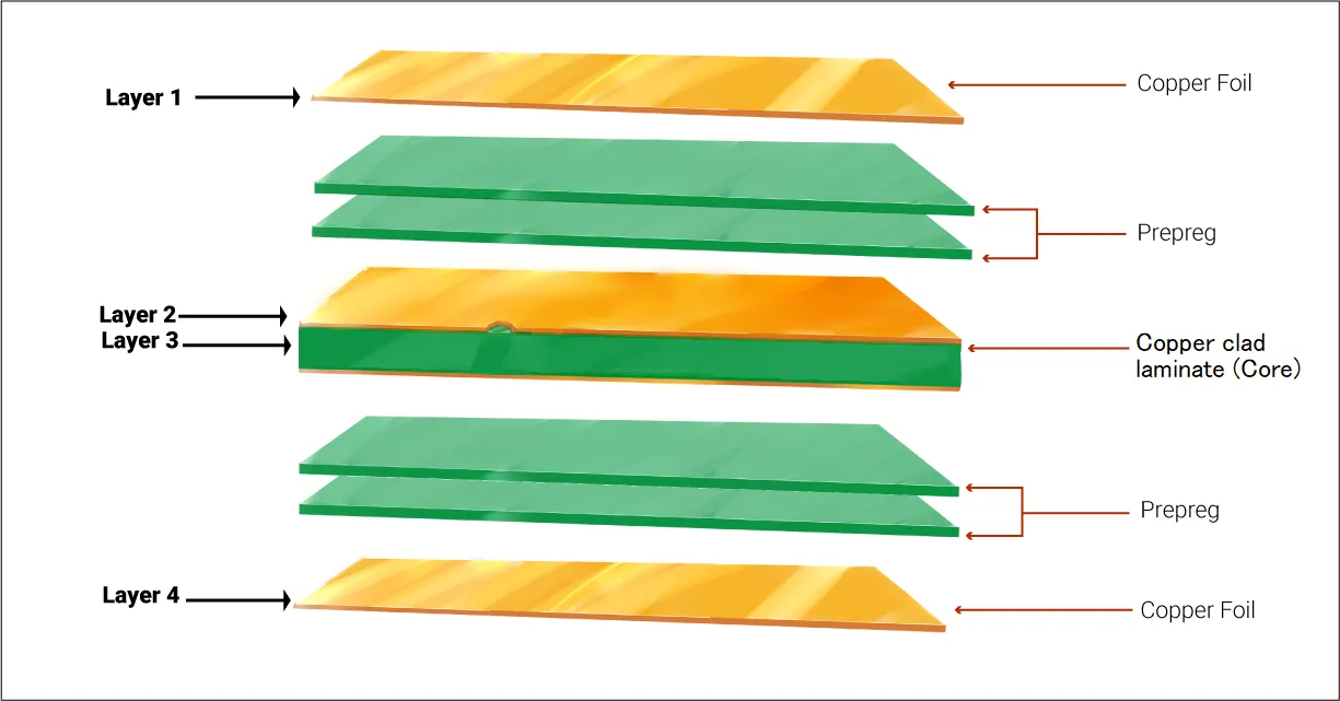
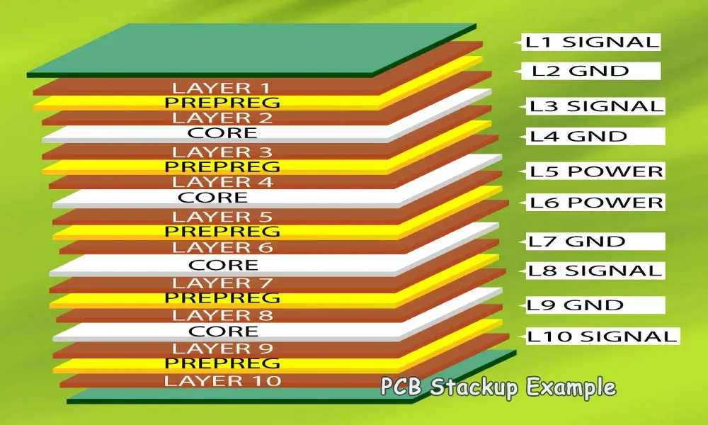
Multilayer PCB 3D Printing: Pushing Design Boundaries
One of the most exciting advancements in this field is multilayer PCB 3D printing. Traditional multilayer boards require complex lamination and drilling processes, but 3D printing simplifies this by building layers directly on top of each other.
This technology enables:
- Compact Designs: By stacking conductive and insulating layers, engineers can fit more functionality into smaller spaces, ideal for compact devices.
- Complex Geometries: 3D printing allows for non-planar multilayer boards, where circuits can wrap around curves or integrate into 3D structures.
- Reduced Production Time: Printing multiple layers in a single process cuts down on assembly steps, often reducing lead times from days to hours.
For example, a multilayer board for a high-speed communication device might include 6 layers with trace widths as small as 0.1 mm, supporting data rates up to 10 Gbps. Achieving this level of precision with traditional methods would be far more time-intensive.
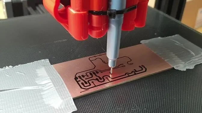
Conductive Ink PCB Printing: Precision and Innovation
Conductive ink PCB printing is at the heart of many 3D printed PCB systems. This technique uses specialized printers to deposit conductive inks in precise patterns, forming the electrical pathways of the board.
Advantages of Conductive Ink Printing
- High Precision: Inkjet systems can achieve resolutions as fine as 20 microns, ensuring accurate trace placement even in dense designs.
- Flexibility: Conductive inks work on a variety of substrates, including flexible and non-planar surfaces, enabling innovative form factors.
- Speed: Printing conductive traces directly eliminates the need for etching, cutting down on production time.
Challenges to Consider
While powerful, conductive ink printing does have limitations. The conductivity of inks is generally lower than solid copper (often by a factor of 10), which can impact performance in high-current applications. Additionally, the durability of printed traces may be lower, requiring protective coatings for long-term use.
Despite these challenges, ongoing advancements in ink formulations are closing the gap, making this method increasingly viable for production beyond just prototyping.
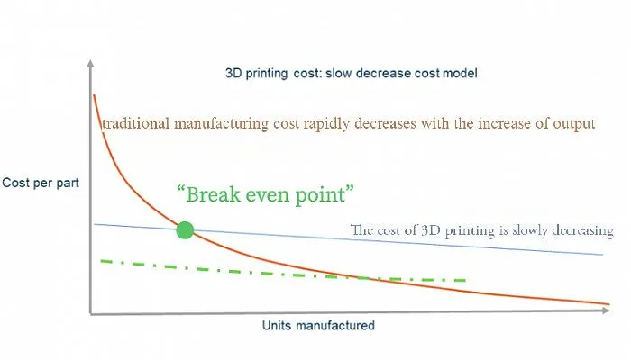
3D PCB Prototyping Cost: What to Expect
Understanding the 3D PCB prototyping cost is essential for engineers considering this technology. While costs can vary based on design complexity, materials, and equipment, here’s a general overview:
- Equipment Costs: Entry-level 3D printers for PCBs start at around $10,000, while industrial-grade systems can exceed $100,000. However, many companies opt for service providers to avoid upfront investments.
- Material Costs: Conductive inks, especially silver-based ones, can cost between $500 and $1,000 per liter. Substrates are more affordable, often ranging from $50 to $200 per kilogram.
- Per-Unit Cost: Prototyping a single small PCB (e.g., 5 cm x 5 cm) might cost between $20 and $100, depending on layer count and material choice. This is often comparable to or cheaper than traditional prototyping for low volumes.
One major cost advantage is the elimination of tooling fees, which can run into thousands of dollars for traditional manufacturing. Additionally, the ability to iterate designs quickly reduces indirect costs related to delays. For instance, a design cycle that traditionally takes 2 weeks might be completed in 1-2 days with 3D printing, saving valuable time.
Benefits of 3D Printing for PCB Prototyping and Manufacturing
Adopting 3D printing for PCBs offers numerous advantages, especially for engineers focused on innovation and speed. Some key benefits include:
- Rapid Prototyping: Print and test designs in hours, not weeks, allowing for faster development cycles.
- Customization: Easily create bespoke designs tailored to specific applications, from flexible wearables to complex multilayer boards.
- Reduced Waste: Additive manufacturing uses only the materials needed, making it a more sustainable option.
- Design Freedom: Experiment with unconventional shapes and structures that traditional methods can’t achieve.
For instance, a startup developing a wearable health monitor could use 3D printing to create a flexible PCB that conforms to the device’s shape, testing multiple iterations in a fraction of the time it would take with conventional processes.
Challenges and Future Outlook for 3D Printed PCBs
While 3D printing for PCBs is revolutionary, it’s not without challenges. Current limitations include lower conductivity compared to copper-clad boards, limited scalability for mass production, and the need for specialized equipment or expertise. However, these hurdles are being addressed through ongoing research.
Looking ahead, advancements in materials—like more conductive and durable inks—and improved printing technologies are set to make 3D printed PCBs viable for larger-scale manufacturing. Industry reports suggest that by 2030, additive manufacturing could account for a significant share of PCB production, especially in niche and custom markets.
How to Get Started with 3D Printing PCBs
If you’re ready to explore 3D printing for your PCB projects, here are some steps to begin:
- Research Equipment: Look into 3D printers designed for electronics, focusing on compatibility with your design software and material needs.
- Choose Materials: Select substrates and conductive inks based on your project’s electrical and mechanical requirements.
- Partner with Experts: For those new to the technology, collaborating with a service provider can simplify the learning curve and reduce costs.
- Test and Iterate: Start with small prototypes, test for performance metrics like signal integrity, and refine your designs as needed.
By leveraging this technology, you can stay ahead in a competitive field, bringing innovative products to market faster.
Conclusion: The Future of PCB Design Is Here
3D printing PCBs is more than just a trend—it’s a game-changer for prototyping and custom manufacturing. From the precision of conductive ink PCB printing to the complexity of multilayer PCB 3D printing, this technology empowers engineers to push boundaries and innovate like never before. While the 3D PCB prototyping cost and material choices require careful consideration, the benefits of speed, customization, and sustainability make it a worthwhile investment.
As advancements continue, the gap between prototyping and production will narrow, making additive manufacturing a cornerstone of electronics design. Whether you’re working on a small project or a groundbreaking device, now is the time to explore how 3D printing can transform your workflow.