ALLPCB


Electroless Nickel Immersion Gold (ENIG) is a widely used surface finish in PCB manufacturing due to its excellent solderability, corrosion resistance, and compatibility with various materials. If you're wondering what materials ENIG can work with, the answer lies in its ability to pair with a range of PCB substrates and conductive metals, particularly copper, which forms the foundation of most PCB designs. ENIG is applied over copper pads and traces to protect them and ensure reliable connections, making it compatible with common PCB base materials like FR-4, polyimide, and even advanced high-frequency laminates.
In this comprehensive guide, we'll dive deeper into the materials that pair well with ENIG, explore how it interacts with different substrates, and provide insights into choosing the right materials for your ENIG PCB construction. Whether you're an engineer designing a high-end circuit board or a manufacturer looking to optimize your process, this blog will help you understand the compatibility of ENIG with various materials.
Understanding ENIG in PCB Construction
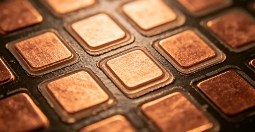
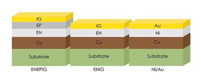
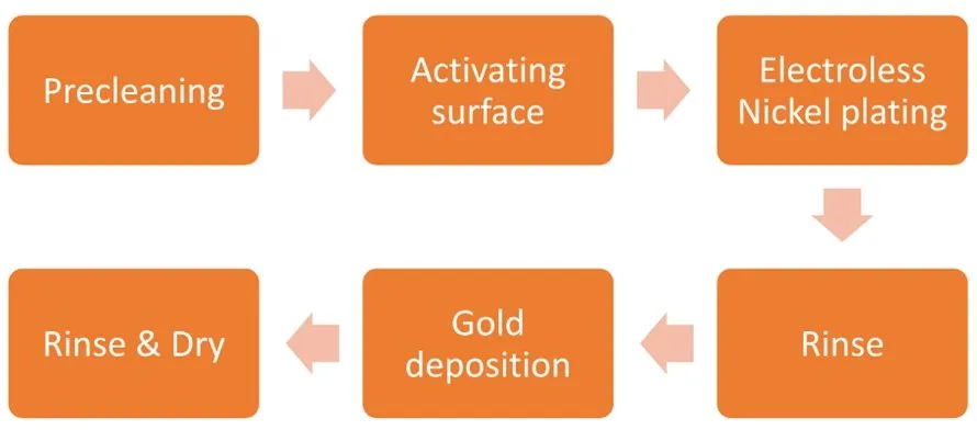
ENIG, or Electroless Nickel Immersion Gold, is a two-layer surface finish applied to the exposed copper surfaces of a printed circuit board (PCB). The process involves depositing a layer of nickel (typically 2 to 6 microns thick) over the copper, followed by a thin layer of gold (usually 0.05 to 0.1 microns). The nickel acts as a barrier to prevent copper diffusion into the gold, while the gold layer ensures excellent solderability and protects against oxidation.
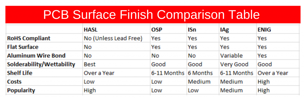
ENIG is a preferred choice for many high-reliability applications, such as 5G communications, aerospace, and medical devices, because of its flat surface, long shelf life, and compatibility with fine-pitch components. However, its performance heavily depends on the underlying materials of the PCB. Let’s explore the materials that work best with ENIG and why.
Core PCB Materials Compatible with ENIG
The base material, or substrate, of a PCB plays a critical role in determining the board’s performance and compatibility with surface finishes like ENIG. Below are the most common PCB materials that work seamlessly with ENIG during construction.
1. FR-4 (Flame Retardant 4)
FR-4 is the most widely used PCB substrate material, made from woven fiberglass cloth and epoxy resin. It is compatible with ENIG due to its stable surface and ability to withstand the chemical processes involved in ENIG plating. FR-4 boards with ENIG finish are often used in consumer electronics, industrial equipment, and automotive applications because of their balance of cost and performance.
ENIG works well with FR-4 because the material’s smooth surface allows for uniform nickel and gold deposition. Additionally, FR-4’s thermal stability (with a glass transition temperature, Tg, typically around 130-140°C for standard grades) ensures it can handle the temperatures involved in ENIG processing and subsequent soldering.
2. High-Tg FR-4
For applications requiring better thermal performance, high-Tg FR-4 (with Tg values of 170-180°C) is a popular choice. This material is often used in high-density interconnect (HDI) boards and multilayer PCBs where heat dissipation is critical. ENIG pairs well with high-Tg FR-4 because the material maintains its structural integrity during the plating process, ensuring a consistent finish.
3. Polyimide
Polyimide is a flexible, high-performance material used in flex and rigid-flex PCBs. It is known for its excellent thermal resistance (withstanding temperatures up to 260°C or higher) and mechanical strength. ENIG is compatible with polyimide substrates, making it a go-to finish for flexible circuits in aerospace, medical, and wearable technology. The gold layer in ENIG provides a reliable surface for soldering components onto flexible polyimide boards without compromising their flexibility.
4. High-Frequency Laminates
High-frequency laminates, such as those made from PTFE (polytetrafluoroethylene) or ceramic-filled materials, are used in RF and microwave applications where low dielectric loss and high signal integrity are essential. These materials often have dielectric constants (Dk) ranging from 2.2 to 3.5 and dissipation factors (Df) as low as 0.0009 at 10 GHz. ENIG works effectively with high-frequency laminates because it provides a flat, conductive surface that minimizes signal loss and supports precise soldering of components.
Conductive Materials and ENIG Compatibility
While the substrate forms the foundation of the PCB, the conductive layers—primarily copper—are where ENIG is directly applied. Let’s look at how ENIG interacts with these materials.
1. Copper
Copper is the primary conductive material in nearly all PCBs, used for traces, pads, and vias. ENIG is specifically designed to work with copper, as the nickel layer acts as a diffusion barrier to prevent copper from mixing with the gold layer, which could degrade solderability. The ENIG process ensures a strong bond with copper, providing a durable and reliable surface for component attachment.
The thickness of the copper layer (typically 1 oz/ft2 or 35 microns for standard boards) does not significantly affect ENIG compatibility, as the plating process adapts to varying copper thicknesses. However, proper surface preparation, such as cleaning and micro-etching, is crucial to ensure uniform ENIG deposition on copper.
2. Other Conductive Materials
While copper is the standard, some specialized PCBs may use alternative conductive materials like aluminum or silver in specific applications. ENIG is generally not applied directly to these materials due to adhesion and compatibility issues. If a PCB design incorporates non-copper conductors, manufacturers often use copper as an intermediary layer before applying ENIG to ensure proper bonding and performance.
Factors to Consider When Choosing Materials for ENIG
Selecting the right materials for ENIG PCB construction involves more than just compatibility. Here are key factors to keep in mind to ensure optimal performance and reliability.
1. Thermal Stability
ENIG processing and subsequent soldering expose the PCB to elevated temperatures. For example, lead-free soldering processes often reach temperatures of 260°C or higher. Materials like standard FR-4 may suffice for less demanding applications, but high-Tg FR-4 or polyimide are better suited for high-temperature environments to prevent delamination or warping during ENIG application.
2. Surface Smoothness
The uniformity of the ENIG finish depends on the smoothness of the underlying material. Rough or uneven surfaces can lead to inconsistent nickel and gold deposition, affecting solderability. FR-4 and high-frequency laminates typically provide a smooth surface, while some low-cost materials may require additional processing to achieve the desired finish quality with ENIG.
3. Application Requirements
The end-use of the PCB dictates material selection. For high-frequency applications, laminates with low dielectric loss are critical, and ENIG supports these materials by providing a low-resistance surface for signal transmission. For flexible circuits, polyimide paired with ENIG ensures durability and reliable connections even under bending stress.
4. Cost Considerations
While ENIG is a premium surface finish, the choice of substrate can significantly impact overall costs. FR-4 is the most cost-effective option for many applications, while high-frequency laminates and polyimide are more expensive but necessary for specialized uses. Balancing material costs with the benefits of ENIG’s reliability is key to optimizing your PCB design.
Advantages of Using ENIG with Compatible Materials
When paired with the right materials, ENIG offers several benefits that enhance PCB performance and longevity. Here are some of the standout advantages:
- Excellent Solderability: The gold layer in ENIG ensures a clean, oxide-free surface for soldering, resulting in strong and reliable joints on materials like FR-4 and polyimide.
- Corrosion Resistance: ENIG protects copper from oxidation, extending the shelf life of PCBs made from various substrates, even in harsh environments.
- Flat Surface: ENIG provides a uniform, flat finish, which is critical for fine-pitch components and high-density designs on high-frequency laminates.
- Compatibility with Multiple Assembly Processes: ENIG supports both leaded and lead-free soldering, wire bonding, and other termination methods, making it versatile across different material types.
Challenges and Limitations
While ENIG is highly compatible with many materials, there are some challenges to be aware of during PCB construction:
- Black Pad Issue: If the nickel layer is not properly applied, a phenomenon called "black pad" can occur, leading to poor solderability. This is more related to the plating process than the material, but choosing a high-quality substrate can minimize risks.
- Cost: ENIG is more expensive than other finishes like HASL (Hot Air Solder Leveling). Pairing it with premium materials like high-frequency laminates can further increase costs.
- Material Preparation: Some substrates may require additional surface treatments before ENIG application to ensure adhesion and uniformity, adding to production time.
Tips for Optimizing ENIG PCB Construction
To get the most out of ENIG with your chosen materials, consider these practical tips:
- Surface Preparation: Ensure the copper surface is clean and free of contaminants before ENIG plating to achieve a uniform finish.
- Material Testing: Conduct compatibility tests with your chosen substrate to verify performance under specific conditions like high temperature or frequency.
- Thickness Control: Monitor nickel and gold layer thicknesses during the ENIG process to meet industry standards (e.g., IPC-4552) and ensure reliability.
- Partner with Experts: Work with a trusted PCB manufacturer to select materials and processes that maximize the benefits of ENIG for your application.
Conclusion
ENIG is a versatile and reliable surface finish that works seamlessly with a wide range of PCB materials, from standard FR-4 to high-performance polyimide and high-frequency laminates. Its primary compatibility lies with copper, the most common conductive material in PCBs, where it provides excellent protection and solderability. By carefully choosing materials for ENIG based on thermal stability, surface smoothness, and application requirements, you can ensure optimal performance for your circuit board designs.
Whether you’re working on consumer electronics, flexible circuits, or high-frequency applications, ENIG offers a robust solution when paired with the right substrate. Understanding the interplay between ENIG and PCB materials empowers engineers and manufacturers to create durable, high-quality boards tailored to their specific needs. With proper material selection and process control, ENIG can elevate the reliability and functionality of your PCB projects.