 ALLPCB


In the world of electronics, power density is a critical factor, especially for high-current applications. If you're searching for ways to boost performance in demanding designs, thick PCBs (Printed Circuit Boards) offer a powerful solution. These boards, often featuring heavy copper layers, excel in handling high currents, managing heat, and ensuring reliability. In this blog post, we'll dive deep into the advantages of thick PCBs, focusing on their current carrying capacity, role in high power PCB design, and thermal management benefits.
Whether you're designing for industrial equipment, automotive systems, or renewable energy solutions, understanding the benefits of thick copper PCBs can transform your projects. Let’s explore why these boards are becoming a go-to choice for engineers tackling high-current challenges.
What Are Thick PCBs and Why Do They Matter?
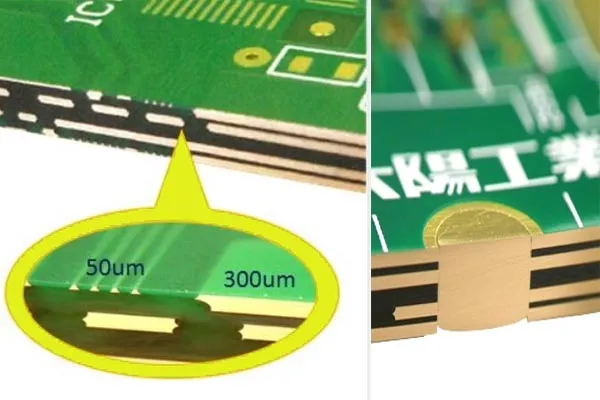
Thick PCBs are circuit boards with copper layers significantly thicker than those found in standard PCBs. While a typical PCB might have copper layers of 1 to 2 ounces per square foot (oz/ft2), thick PCBs often feature copper weights of 3 oz/ft2 or more, sometimes reaching up to 20 oz/ft2 in extreme cases. This increased thickness directly enhances the board's ability to carry higher currents without overheating or failing.
In high-current applications, such as power supplies or motor controllers, standard PCBs often struggle with heat buildup and electrical resistance. Thick PCBs address these issues head-on, offering a robust foundation for power-dense designs. Their importance lies in their ability to support modern electronics where efficiency and reliability are non-negotiable.
Key Advantages of Thick PCBs in High-Current Applications
Thick PCBs bring a range of benefits to the table, especially when dealing with high power demands. Below, we break down the core advantages that make these boards indispensable for engineers.
1. Superior Thick PCB Current Carrying Capacity
One of the standout features of thick PCBs is their exceptional current carrying capacity. The thicker copper layers reduce electrical resistance, allowing more current to flow through the traces without significant voltage drops or overheating. For instance, a 1 oz/ft2 copper trace might safely carry around 1-2 amps depending on width, while a 10 oz/ft2 trace can handle upwards of 20-30 amps under similar conditions.
This capability is crucial in applications like electric vehicle (EV) chargers or industrial inverters, where currents can spike to hundreds of amps. By using thick PCBs, designers can minimize the risk of trace burnout and ensure stable performance even under heavy loads.
2. Enhanced Thermal Management with Thick PCBs
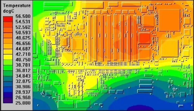
Heat dissipation is a major concern in high power PCB design. When current flows through a conductor, it generates heat due to resistance. In standard PCBs, this heat can accumulate, leading to component failure or reduced lifespan. Thick PCBs, however, excel in thermal management thanks to their heavy copper layers, which act as natural heat sinks.
Copper is an excellent conductor of heat, with a thermal conductivity of about 400 W/m·K. Thicker layers spread heat more effectively across the board, preventing hotspots. This is particularly valuable in compact designs where space for additional cooling solutions like fans or heat sinks is limited. For example, in a power converter operating at 50 amps, a thick PCB can reduce peak temperatures by as much as 20-30°C compared to a standard board, significantly improving reliability.
3. Durability and Mechanical Strength
Thick PCBs are not just about electrical performance; they also offer superior mechanical strength. The added copper weight makes the board more robust, reducing the risk of cracking or delamination under physical stress or thermal cycling. This durability is essential in harsh environments, such as automotive or aerospace applications, where boards are exposed to vibration, shock, and temperature swings.
For instance, in an automotive power module, a thick PCB can withstand repeated thermal expansion and contraction without developing solder joint cracks. This reliability translates to longer product lifespans and fewer maintenance issues, saving both time and cost in the long run.
4. Reduced Voltage Drop and Improved Efficiency
In high-current circuits, voltage drop across traces can lead to inefficiencies and performance issues. Thick copper PCB benefits include lower resistance, which minimizes voltage drop and ensures that more power reaches the intended components. This is especially important in applications like solar inverters, where even a small loss in efficiency can impact overall system performance.
By using a thick PCB with 6 oz/ft2 copper, for example, a designer can reduce resistance by nearly 80% compared to a 1 oz/ft2 board for the same trace width. This improvement not only boosts efficiency but also reduces energy waste, aligning with the growing demand for sustainable electronics.
Applications of Thick PCBs in High Power Design
Thick PCBs are a game-changer across various industries where high power and reliability are paramount. Here are some key areas where these boards shine.
Automotive and Electric Vehicles
The rise of electric vehicles has driven demand for high power PCB design. Components like battery management systems (BMS) and DC-DC converters handle currents ranging from 50 to 200 amps. Thick PCBs provide the necessary current carrying capacity and thermal management to ensure these systems operate safely and efficiently, even under the extreme conditions of an EV powertrain.
Renewable Energy Systems
In solar and wind energy systems, inverters and power controllers must manage high currents while maintaining efficiency. Thick PCBs help by reducing power losses and dissipating heat effectively, ensuring that renewable energy systems deliver maximum output without overheating.
Industrial Equipment
Heavy machinery and industrial power supplies often operate at high currents and voltages. Thick PCBs are ideal for motor drives and power distribution boards, offering the durability and performance needed to keep equipment running smoothly in demanding factory environments.
Design Considerations for Thick PCBs in High-Current Applications
While thick PCBs offer numerous advantages, designing with them requires careful planning. Here are some key factors to keep in mind to maximize their benefits.
Trace Width and Spacing
Even with thick copper, trace width must be calculated based on the expected current load. Wider traces reduce resistance and heat buildup. Industry standards, such as IPC-2221, provide guidelines for determining trace width based on current and copper thickness. For a 10 oz/ft2 copper layer carrying 20 amps, a trace width of at least 0.1 inches might be necessary to keep temperature rise below 10°C.
Layer Stack-Up and Via Design
In multilayer thick PCBs, proper via design is critical for current distribution and heat dissipation. Using multiple vias or larger via sizes can improve thermal conductivity and reduce resistance between layers. This is especially important in designs where current must pass through several layers to reach components.
Material Selection
The substrate material plays a big role in thermal management for thick PCBs. High-Tg (glass transition temperature) materials or metal-core substrates can enhance heat dissipation and mechanical stability. For instance, a metal-core PCB with a copper base can offer thermal conductivity up to 10 times higher than standard FR-4 materials, making it ideal for extreme high-current designs.
Challenges of Using Thick PCBs and How to Overcome Them
Despite their benefits, thick PCBs come with certain challenges. Understanding these hurdles and how to address them is key to successful implementation.
Higher Manufacturing Costs
The increased copper weight and specialized manufacturing processes for thick PCBs can drive up costs. However, the long-term benefits of improved reliability and reduced failure rates often outweigh the initial investment. Partnering with a trusted manufacturer can also help optimize costs without compromising quality.
Weight and Size Constraints
Thick PCBs are heavier and may not suit applications where weight is a critical factor, such as portable devices. In such cases, designers can explore hybrid solutions, using thick copper only in high-current sections while keeping other areas lightweight.
Etching and Fabrication Complexity
Thicker copper layers are harder to etch precisely, which can lead to manufacturing challenges. Working with experienced fabrication partners who specialize in heavy copper boards ensures that traces and features are accurately produced, maintaining design integrity.
How Thick PCBs Drive Innovation in High Power Electronics
As electronics continue to evolve, the demand for higher power density pushes the boundaries of PCB technology. Thick PCBs are at the forefront of this innovation, enabling designs that were once impossible due to thermal and electrical limitations. From supporting the electrification of transportation to powering renewable energy grids, these boards are unlocking new possibilities for engineers.
By leveraging the thick PCB current carrying capacity and thermal management advantages, designers can create compact, efficient, and reliable systems. This not only improves product performance but also aligns with global trends toward sustainability and energy efficiency.
Conclusion: Why Choose Thick PCBs for Your Next High-Current Project?
Thick PCBs are a powerful tool for tackling the challenges of high-current applications. Their ability to handle substantial currents, manage heat effectively, and withstand harsh conditions makes them an ideal choice for industries ranging from automotive to industrial power systems. The thick copper PCB benefits—such as reduced voltage drop, enhanced durability, and superior thermal management—translate directly into better performance and longer-lasting designs.
At ALLPCB, we’re committed to helping engineers harness the full potential of thick PCBs in high power PCB design. Whether you’re working on a cutting-edge EV system or a robust industrial controller, incorporating these boards into your projects can elevate your results. Embrace the power of thick PCBs and unlock new levels of efficiency and reliability in your next design.


