ALLPCB


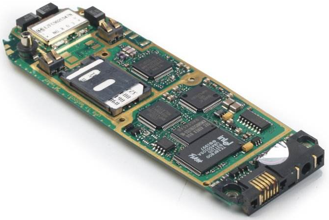
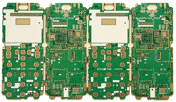
In the fast-paced world of mobile technology, every millimeter of space counts. As devices become smaller yet more powerful, the demand for compact, high-density PCB designs has skyrocketed. One game-changing innovation helping to meet this demand is the use of buried resistors in mobile device PCBs. But what exactly are buried resistors, and how do they contribute to PCB miniaturization and high-density PCB design? Simply put, buried resistors are components embedded within the layers of a printed circuit board (PCB), freeing up surface space and enabling tighter, more efficient designs for mobile devices.
In this blog post, we’ll dive deep into the world of buried resistors for mobile devices, exploring how they save space, enhance performance, and revolutionize high-density PCB design. Whether you’re an engineer looking to optimize your next project or a tech enthusiast curious about the inner workings of your smartphone, this guide will provide valuable insights into buried resistor space-saving techniques and their impact on modern electronics.
What Are Buried Resistors and Why Do They Matter?
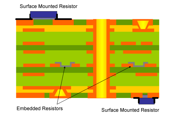
Buried resistors are resistive elements integrated directly into the inner layers of a PCB, rather than being mounted on the surface like traditional resistors. This placement allows designers to utilize the surface area of the board for other critical components, such as processors, sensors, or connectors, which are essential in mobile devices. Unlike surface-mounted resistors that take up valuable real estate, buried resistors are “hidden” within the board’s structure, making them a key player in PCB miniaturization.
The importance of buried resistors in mobile devices cannot be overstated. As smartphones, wearables, and other portable gadgets continue to shrink in size, the need for high-density PCB design grows. These resistors help reduce the overall footprint of the board while maintaining or even improving electrical performance. By embedding resistors, manufacturers can achieve cleaner layouts, shorter signal paths, and reduced electromagnetic interference (EMI), all of which are critical for the high-speed operations of modern mobile devices.
The Role of Buried Resistors in PCB Miniaturization
PCB miniaturization is the process of designing smaller, more compact circuit boards without sacrificing functionality. In mobile devices, where space is at a premium, miniaturization is a top priority. Buried resistors play a pivotal role in this process by eliminating the need for surface-mounted components, thus allowing for a higher density of components in a smaller area.
For example, consider a typical smartphone PCB, which may need to accommodate hundreds of components in a space no larger than a few square inches. By integrating resistors into the board’s layers, designers can reduce the board’s surface area by up to 20-30%, depending on the complexity of the design. This space saving is crucial for fitting advanced features like larger batteries, additional cameras, or enhanced processors into the slim form factors of modern devices.
Moreover, buried resistors contribute to thinner PCBs. Traditional surface-mounted resistors add height to the board, which can be a limiting factor in ultra-thin devices like smartwatches or foldable phones. By embedding resistors, the overall stack-up height of the PCB can be reduced, supporting the trend toward sleeker, lighter mobile devices.
Advantages of Buried Resistors in High-Density PCB Design
High-density PCB design focuses on packing as many components and connections as possible into a limited space. Buried resistors offer several advantages that make them ideal for this approach, especially in mobile devices. Let’s break down some of the key benefits:
- Space Efficiency: As mentioned, buried resistors free up surface space, allowing for more components or a smaller overall board size. This is a critical factor in achieving buried resistor space saving for mobile devices.
- Improved Signal Integrity: By placing resistors closer to the components they serve, buried resistors reduce the length of signal paths. Shorter paths mean less signal delay and lower chances of interference, which is vital for high-speed data transfer in 5G-enabled devices. For instance, signal delays can be reduced by as much as 10-15% in designs using embedded components.
- Reduced EMI: Electromagnetic interference is a common challenge in densely packed mobile device PCBs. Buried resistors, being embedded within the board, are naturally shielded by the surrounding layers, minimizing EMI and ensuring stable performance even in compact layouts.
- Enhanced Reliability: Since buried resistors are protected within the PCB layers, they are less exposed to environmental factors like moisture, dust, or physical damage. This leads to improved durability, which is essential for mobile devices that face constant handling and varying conditions.
How Buried Resistors Enhance Performance in Mobile Devices
Beyond space savings, buried resistors offer performance benefits that directly impact the functionality of mobile devices. One major advantage is their ability to support precise impedance control. In high-frequency applications, such as 5G connectivity or Wi-Fi 6, maintaining consistent impedance is crucial for signal integrity. Buried resistors can be designed with tight tolerance values, often within ±1% of the target resistance, ensuring reliable performance in these demanding scenarios.
Additionally, buried resistors help manage heat dissipation in compact designs. Mobile devices generate significant heat due to powerful processors and constant usage. By embedding resistors within the board, heat distribution can be better managed across the layers, reducing hotspots on the surface. This can extend the lifespan of the device and prevent performance throttling due to overheating.
Another performance boost comes from the reduction in parasitic effects. Surface-mounted resistors often introduce unwanted capacitance or inductance due to their physical placement and lead connections. Buried resistors, integrated directly into the PCB material, minimize these parasitic effects, leading to cleaner signal transmission and improved overall efficiency.
Challenges and Considerations in Using Buried Resistors
While buried resistors offer numerous advantages for PCB miniaturization and high-density PCB design, they are not without challenges. Understanding these considerations is essential for engineers looking to implement this technology in mobile devices.
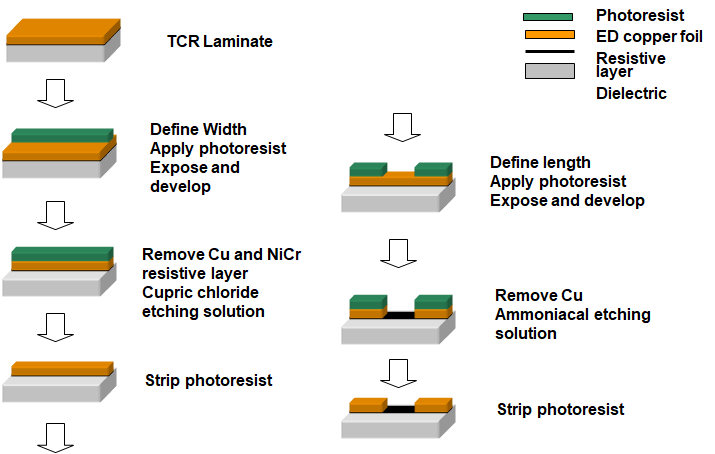
One primary challenge is the complexity of manufacturing. Embedding resistors within PCB layers requires advanced fabrication techniques, such as precise laser trimming or specialized resistive materials. This can increase production costs, especially for prototypes or small-batch runs. However, as technology advances and adoption grows, these costs are expected to decrease.
Another consideration is design flexibility. Once buried resistors are integrated into the PCB, they cannot be easily replaced or adjusted like surface-mounted components. This means that designs must be thoroughly tested and validated before manufacturing to avoid costly revisions. Engineers often use simulation tools to predict performance and ensure that resistance values—typically ranging from 10 ohms to 1 megaohm—meet the circuit’s requirements.
Lastly, thermal management during manufacturing must be carefully controlled. The process of embedding resistors involves high temperatures, which can affect the integrity of other materials in the PCB. Proper material selection, such as using high-Tg (glass transition temperature) laminates, can mitigate these risks and ensure a reliable final product.
Applications of Buried Resistors in Mobile Devices
Buried resistors are already making a significant impact in various mobile device applications, driving innovation in design and functionality. Here are a few key areas where they are being utilized:
- Smartphones and Tablets: These devices require compact, high-density PCBs to support advanced features like multiple cameras, larger displays, and faster processors. Buried resistors enable designers to pack more functionality into smaller spaces, supporting the trend toward bezel-less designs and foldable screens.
- Wearable Technology: Devices like smartwatches and fitness trackers have extremely limited space for electronics. Buried resistors allow for ultra-compact PCB designs, ensuring that these wearables remain lightweight and comfortable while delivering powerful performance.
- IoT Devices: Internet of Things (IoT) gadgets, such as smart home sensors or connected earbuds, benefit from buried resistor space saving. Their small form factors often leave little room for traditional components, making embedded resistors an ideal solution.
By leveraging buried resistors, manufacturers can push the boundaries of what’s possible in mobile device design, creating products that are not only smaller but also more efficient and reliable.
Future Trends: The Evolution of Buried Resistors in PCB Design
As technology continues to evolve, so too will the role of buried resistors in high-density PCB design. One emerging trend is the integration of other passive components, such as capacitors and inductors, into PCB layers. This concept, known as embedded passives, could further enhance PCB miniaturization, reducing surface component counts by up to 50% in some designs.
Another exciting development is the use of advanced materials for buried resistors. New resistive inks and thin-film technologies are being explored to achieve even tighter tolerances and higher reliability. These innovations could lead to resistors with resistance values as precise as ±0.5%, opening up new possibilities for high-performance mobile devices.
Additionally, the rise of 5G and beyond will drive demand for buried resistors in mobile devices. As data speeds increase—potentially reaching 10 Gbps or more with future networks—signal integrity and EMI reduction will become even more critical. Buried resistors, with their ability to minimize interference and optimize signal paths, will be at the forefront of this technological shift.
Conclusion: Embracing Buried Resistors for Next-Gen Mobile Devices
The push for smaller, more powerful mobile devices shows no signs of slowing down, and buried resistors are proving to be a vital tool in meeting this challenge. By enabling PCB miniaturization and supporting high-density PCB design, these embedded components help save space, improve performance, and enhance reliability in everything from smartphones to wearables. The advantages of buried resistor space saving are clear, offering engineers the freedom to innovate without the constraints of traditional surface-mounted components.
As manufacturing techniques improve and new materials emerge, the adoption of buried resistors in mobile devices will only grow. For designers and manufacturers, staying ahead of the curve means embracing this technology to create cutting-edge products that meet the demands of today’s tech-savvy consumers. At ALLPCB, we’re committed to supporting this revolution with advanced solutions for high-density PCB design, helping bring your compact, high-performance designs to life.