 ALLPCB


In the fast-paced world of electronics, ensuring signal integrity in high-speed PCB designs is more important than ever. If you're working on complex projects with a 16-layer PCB, maintaining clear and reliable signals can be a challenge. So, how do you optimize signal integrity for high-speed designs using 16-layer PCBs? The key lies in careful planning, precise impedance control, effective crosstalk reduction, and leveraging simulation tools to predict and address issues before they arise.
In this blog, we'll dive deep into the essentials of 16-layer PCB signal integrity, explore best practices for high-speed PCB design, and provide actionable tips on impedance control, crosstalk reduction, and signal integrity simulation. Whether you're an experienced engineer or new to multilayer PCB design, this guide will help you achieve reliable performance in your projects.
Why Signal Integrity Matters in High-Speed PCB Design
Signal integrity refers to the quality of an electrical signal as it travels through a printed circuit board. In high-speed designs, where data rates can exceed several gigabits per second (Gbps), even small distortions can lead to errors, data loss, or system failure. With a 16-layer PCB, the complexity increases due to the number of layers, tight spacing, and multiple signal paths, making signal integrity a top priority.
Issues like crosstalk, signal reflection, and electromagnetic interference (EMI) can degrade performance. For example, in a design operating at 10 Gbps, a slight mismatch in impedance could cause reflections that disrupt data transmission. By focusing on signal integrity from the start, you can avoid costly redesigns and ensure your product meets performance expectations.
Understanding the Challenges of 16-Layer PCB Signal Integrity
A 16-layer PCB offers significant advantages for high-speed designs, such as increased routing density and better separation of power and signal planes. However, it also introduces unique challenges:
- Complex Layer Stack-Up: With 16 layers, managing the arrangement of signal, power, and ground planes is critical to minimize noise and interference.
- High-Density Routing: Tight spacing between traces can lead to crosstalk, where signals on adjacent traces interfere with each other.
- Impedance Mismatches: Variations in trace width, dielectric materials, or layer transitions can cause signal reflections.
- Thermal and Power Distribution: High-speed signals generate heat, and uneven power distribution across layers can introduce noise.
Addressing these challenges requires a systematic approach to design, simulation, and testing. Let’s explore the key strategies to optimize 16-layer PCB signal integrity.
Key Strategies for High-Speed PCB Design with 16-Layer Boards
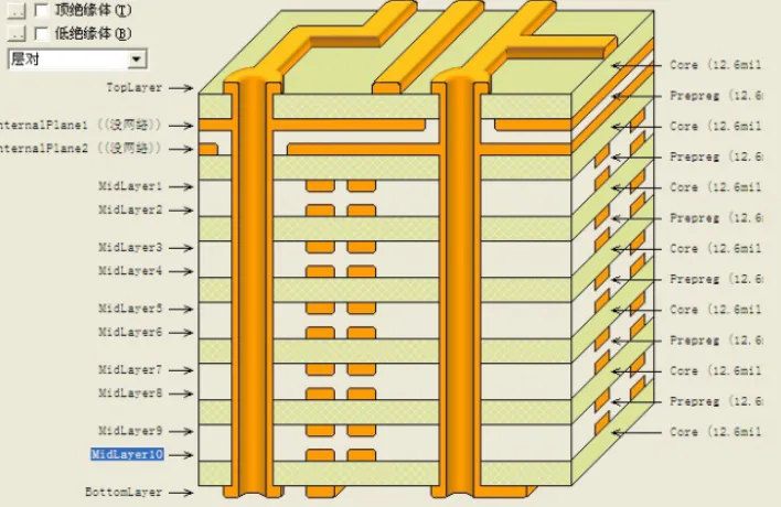
1. Design an Effective Layer Stack-Up
The foundation of signal integrity in a 16-layer PCB is a well-planned layer stack-up. A typical stack-up for high-speed designs might include multiple ground and power planes sandwiching signal layers to provide shielding and stable reference planes. For instance:
- Layers 1 and 16: Top and bottom signal layers for external components.
- Layers 2, 4, 6, 8, 10, 12, 14: Ground planes or power planes for noise isolation.
- Layers 3, 5, 7, 9, 11, 13, 15: Signal layers for high-speed traces.
This configuration helps reduce EMI by ensuring that high-speed signals are routed between ground planes, creating a controlled environment for signal propagation. Keep the dielectric thickness consistent between layers to maintain uniform impedance, typically in the range of 3 to 5 mils for high-speed applications.
2. Implement Impedance Control for Signal Paths
Impedance control is a cornerstone of high-speed PCB design. Impedance mismatches can cause signal reflections, leading to data errors. For a 16-layer PCB, achieving consistent impedance requires precise control over trace width, spacing, and dielectric properties.
For example, a common target impedance for high-speed signals like USB 3.0 or PCIe is 50 ohms for single-ended traces or 100 ohms for differential pairs. Use the following guidelines:
- Calculate trace width and spacing using impedance calculators based on your PCB material (e.g., FR-4 with a dielectric constant of 4.2).
- Maintain uniform trace geometry across layers to avoid variations.
- Use reference planes (ground or power) directly below signal traces to create a stable return path.
By prioritizing impedance control, you can minimize reflections and ensure clean signal transmission at speeds exceeding 5 Gbps.
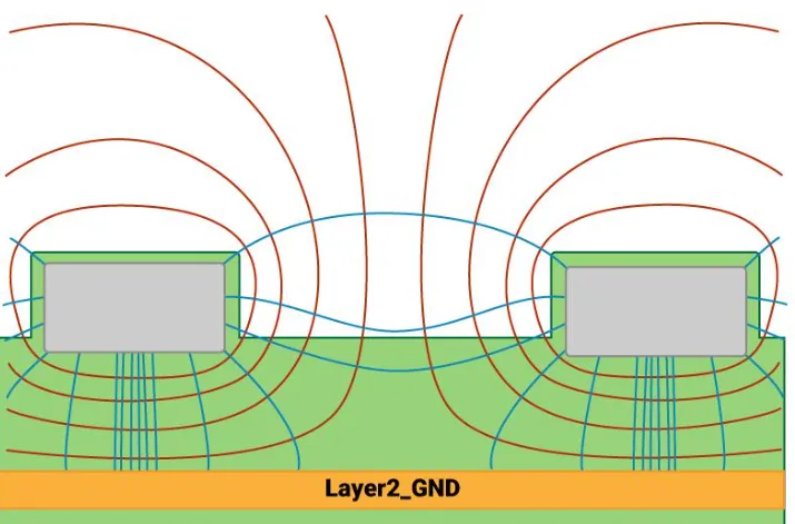
3. Minimize Crosstalk in High-Density Designs
Crosstalk reduction is vital in a 16-layer PCB where traces are closely spaced. Crosstalk occurs when signals on adjacent traces or layers interfere with each other, causing noise and timing errors. To mitigate this:
- Increase spacing between high-speed traces. A general rule is to keep spacing at least 3 times the trace width (3W rule).
- Route high-speed signals on different layers, separated by ground planes to act as shields.
- Use differential signaling for critical data paths, as it inherently cancels out noise and reduces crosstalk.
For instance, in a design with DDR4 memory operating at 3200 MHz, routing address and data lines on separate layers with ground plane separation can reduce crosstalk by up to 30% compared to routing on the same layer.
4. Leverage Signal Integrity Simulation Tools
Before manufacturing a 16-layer PCB, conducting signal integrity simulation is a must for high-speed designs. Simulation tools allow you to model signal behavior, identify potential issues, and optimize your layout without costly prototypes.
Key aspects to simulate include:
- Eye Diagrams: Assess signal quality and timing margins at data rates like 10 Gbps to ensure clear signal transitions.
- Reflection Analysis: Detect impedance mismatches that could cause signal bounce-back.
- Crosstalk Analysis: Evaluate interference between traces and adjust spacing or routing as needed.
By running simulations early in the design phase, you can catch issues like a 5% impedance mismatch that might degrade signal quality at high frequencies, saving time and resources during production.
5. Optimize Power Distribution and Grounding
A stable power delivery network (PDN) is essential for signal integrity. Voltage fluctuations or noise on power planes can couple into signal lines, especially in a 16-layer PCB with multiple power domains. Follow these practices:
- Dedicate multiple layers to ground planes to provide low-impedance return paths for signals.
- Place decoupling capacitors (e.g., 0.1 μF and 1 μF) near high-speed ICs to filter noise, with placement within 100 mils of power pins.
- Minimize via transitions for high-speed signals to reduce inductance and maintain signal integrity.
A well-designed PDN can reduce power supply noise by up to 20 dB, significantly improving signal quality in high-speed applications.
Practical Tips for Implementing High-Speed PCB Design
Beyond the core strategies, here are some practical tips to fine-tune your 16-layer PCB for optimal signal integrity:
- Route Critical Signals First: Prioritize high-speed traces like clock lines or data buses before routing less critical signals to ensure optimal paths.
- Avoid 90-Degree Bends: Use 45-degree angles or curved traces to prevent signal reflections caused by sharp corners.
- Match Trace Lengths: For differential pairs or parallel buses, keep trace lengths within 5 mils of each other to avoid timing skew.
- Choose the Right Materials: Opt for low-loss dielectric materials with a dissipation factor (Df) below 0.01 for frequencies above 1 GHz.
These small adjustments can make a big difference, especially when dealing with data rates of 10 Gbps or higher.

Common Pitfalls to Avoid in 16-Layer PCB Design
Even with the best intentions, mistakes can compromise signal integrity. Watch out for these common pitfalls:
- Ignoring Via Effects: Excessive vias in high-speed signal paths can introduce inductance and capacitance, degrading signals. Limit vias to 1-2 per net for critical traces.
- Overlooking Return Paths: Ensure every signal has a continuous return path on an adjacent ground plane to avoid loop inductance.
- Neglecting Thermal Management: High-speed signals generate heat, so incorporate thermal vias and heat sinks to prevent performance degradation.
By staying mindful of these issues, you can prevent signal integrity problems before they impact your design.
Conclusion: Achieving Excellence in High-Speed PCB Design
Optimizing 16-layer PCB signal integrity for high-speed PCB design requires a combination of strategic planning, precise execution, and advanced tools. By focusing on layer stack-up, impedance control, crosstalk reduction, and signal integrity simulation, you can build reliable and high-performing boards for even the most demanding applications.
Start with a solid foundation by designing an effective stack-up and controlling impedance. Use simulation tools to predict and resolve issues early, and apply best practices like proper grounding and crosstalk mitigation to ensure clean signals. With these steps, your 16-layer PCB will be ready to handle high-speed data rates with minimal distortion or noise.
At ALLPCB, we’re committed to supporting your journey in high-speed design. By applying the techniques in this guide, you’ll be well-equipped to tackle the challenges of multilayer boards and deliver top-notch performance in your electronic projects.


