 ALLPCB


If you're dealing with solder mask misregistration or alignment problems in PCB manufacturing, you're not alone. These issues can lead to exposed copper, shorts, or assembly failures. The good news? Most solder mask registration issues can be fixed with the right approach. In this blog, we'll dive deep into the causes of solder mask misregistration and provide practical solutions to help you achieve flawless PCB production.
What Is Solder Mask Registration and Why Does It Matter?
Solder mask registration refers to the precise alignment of the solder mask layer over the copper traces and pads on a printed circuit board (PCB). The solder mask, a protective coating, insulates the copper, prevents solder bridges during assembly, and shields the board from environmental damage like oxidation. When misregistration occurs, the solder mask doesn't align correctly with the underlying features, exposing copper or covering areas meant for soldering.
Why is this a problem? Misaligned solder masks can cause electrical shorts, poor solder joints, or even complete board failure during assembly. For high-density designs, even a small offset of 0.05 mm can lead to significant issues, especially with fine-pitch components. Understanding and fixing solder mask registration is critical for ensuring reliability and performance in PCB manufacturing.
Common Causes of Solder Mask Misregistration
Before diving into solutions, let’s explore the root causes of solder mask alignment problems. Identifying the source of the issue is the first step to preventing it in future designs or production runs.
1. Artwork and Design File Errors
One of the most frequent causes of solder mask misregistration starts at the design stage. If the solder mask layer in your design files isn't perfectly aligned with the copper layer, the misalignment will carry over to manufacturing. This can happen due to incorrect layer scaling, improper export settings, or even manual errors during file preparation. For instance, a scaling mismatch of just 1% can result in a noticeable offset across a large board.
2. Manufacturing Process Variations
During PCB fabrication, small variations in equipment calibration or material properties can lead to alignment issues. For example, the photolithography process used to apply the solder mask relies on precise alignment of photomasks. If the equipment isn’t calibrated correctly, or if there’s thermal expansion in the PCB substrate (often up to 0.02% per degree Celsius), the solder mask may shift relative to the copper features.
3. Material Shrinkage or Expansion
PCB substrates and solder mask materials can expand or contract due to temperature and humidity changes during manufacturing. FR-4, a common PCB material, has a thermal expansion coefficient of about 14-17 ppm/°C. If the solder mask material doesn’t match this behavior, or if curing temperatures aren’t controlled, misregistration can occur. This is especially problematic in multi-layer boards where alignment must be maintained across several layers.
4. Insufficient Solder Mask Clearance
Inadequate clearance between the solder mask openings and copper pads can amplify the appearance of misregistration. If the design specifies a clearance of only 0.05 mm, even a slight offset of 0.02 mm can expose copper or cover part of the pad. This not only affects aesthetics but also functionality during soldering.

5. Human Error and Quality Control
Manual handling or inadequate quality checks during production can also contribute to alignment problems. For instance, if operators misalign panels during the solder mask application process, or if inspection steps are skipped, small errors can go unnoticed until it’s too late.
Impact of Solder Mask Alignment Problems on PCB Performance
Solder mask misregistration isn’t just a cosmetic issue; it can have serious consequences for your PCB’s functionality and reliability. Here are some common outcomes:
- Exposed Copper: Misaligned solder mask can leave copper traces or pads exposed, leading to oxidation or unintended solder bridges during assembly.
- Soldering Issues: If the mask covers part of a pad, it can prevent proper solder adhesion, resulting in weak or failed joints.
- Electrical Shorts: Exposed adjacent traces, especially under fine-pitch components, increase the risk of shorts, which can cause circuit failure.
- Assembly Delays: Boards with registration errors often require rework or rejection, leading to production delays and increased costs.
These issues are particularly critical in high-reliability applications like automotive or medical electronics, where even a 0.1 mm offset can compromise safety and performance.
Solutions for Fixing Solder Mask Registration Issues
Now that we’ve covered the causes and impacts of solder mask misregistration, let’s focus on actionable solutions to address and prevent these problems. Whether you’re a designer or manufacturer, these steps can help ensure precise alignment.
1. Optimize Design Files for Accuracy
Start by double-checking your design files before sending them to production. Use design software tools to verify that the solder mask layer aligns perfectly with the copper layer. Set appropriate clearances—typically 0.1 mm to 0.15 mm around pads—to account for minor manufacturing tolerances. Export files in a high-resolution format to avoid scaling errors, and always include registration marks or fiducials in your design to assist with alignment during fabrication.
2. Collaborate with Your Manufacturer
Clear communication with your PCB fabrication partner is essential. Provide detailed documentation, including layer stack-up information and alignment requirements. Request a design for manufacturability (DFM) review to catch potential issues before production begins. Many manufacturers also offer tighter registration tolerances (e.g., ±0.05 mm) for an additional cost—consider this for high-precision designs.
3. Control Manufacturing Environment
For manufacturers, maintaining a stable production environment is key to preventing material expansion or shrinkage. Control temperature and humidity in the fabrication area to minimize thermal effects on PCB substrates and solder mask materials. Regularly calibrate equipment used for photolithography and solder mask application to ensure alignment accuracy within 0.025 mm or better.
4. Use High-Quality Materials
Choose solder mask materials with thermal and mechanical properties that match your PCB substrate. Liquid photoimageable (LPI) solder masks, for example, offer better registration accuracy compared to dry film masks due to their ability to conform to surface variations. Ensure that curing processes are optimized to avoid uneven shrinkage—typical curing temperatures range from 120°C to 150°C, depending on the material.
5. Implement Strict Quality Control
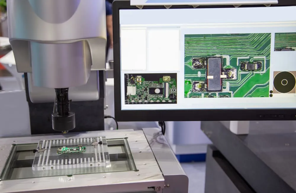
Incorporate automated optical inspection (AOI) systems to detect solder mask misregistration early in the production process. AOI can identify offsets as small as 0.01 mm, allowing for immediate corrective action. Additionally, perform manual inspections on a sample of boards from each batch to ensure consistency. If misregistration is detected, analyze the root cause using data from the inspection to prevent recurrence.
6. Adjust Solder Mask Clearances for Tolerance
If tight registration tolerances aren’t feasible due to cost or equipment limitations, consider increasing solder mask clearances in your design. A clearance of 0.2 mm instead of 0.1 mm provides more room for minor misalignments without exposing copper or covering pads. While this may slightly alter the board’s appearance, it can significantly reduce the risk of functional issues.
Preventing PCB Manufacturing Errors Related to Solder Mask
While troubleshooting existing issues is important, prevention is always better than correction. Here are some best practices to minimize solder mask alignment problems in future projects:
- Standardize Design Guidelines: Create a set of design rules that account for manufacturing tolerances, such as minimum solder mask clearances and alignment marks.
- Prototype and Test: Before full-scale production, fabricate a small batch of boards to identify potential registration issues. Use this feedback to refine your design or process.
- Invest in Training: Ensure that design and manufacturing teams are trained in best practices for solder mask application and alignment.
- Update Equipment: Use modern machinery with high-precision alignment capabilities to reduce variability in the solder mask process.
Case Study: Solving Solder Mask Misregistration in a High-Density Design
Consider a real-world scenario where a high-density PCB for a consumer electronics device encountered solder mask misregistration. The design featured 0.5 mm pitch components, and an offset of 0.08 mm caused exposed traces near critical pads, leading to assembly failures in 15% of the initial batch.
The solution involved multiple steps. First, the design team increased the solder mask clearance from 0.1 mm to 0.15 mm to accommodate manufacturing tolerances. Next, they added fiducial marks at the board corners to improve alignment during production. The manufacturer recalibrated their photolithography equipment and implemented stricter temperature controls (maintaining a range of 22°C to 25°C) during solder mask curing. Finally, AOI was used to inspect every board in the revised batch. The result? Misregistration issues dropped to under 1%, and assembly yield improved significantly.
This example shows how a combination of design adjustments, process controls, and quality checks can effectively address solder mask alignment problems.
Conclusion: Mastering Solder Mask Registration for Flawless PCBs
Solder mask misregistration is a common challenge in PCB manufacturing, but it doesn’t have to derail your project. By understanding the causes—such as design errors, material variations, and process inconsistencies—you can take proactive steps to fix and prevent these issues. From optimizing your design files to implementing strict quality controls, the solutions outlined in this guide offer practical ways to ensure precise solder mask alignment.
Whether you're dealing with exposed copper, soldering defects, or assembly delays due to solder mask alignment problems, the key is to address the issue early through collaboration, testing, and process improvement. With these strategies, you can achieve reliable, high-quality PCBs that meet even the most demanding specifications. Let’s build better boards together by tackling solder mask registration head-on.


