 ALLPCB


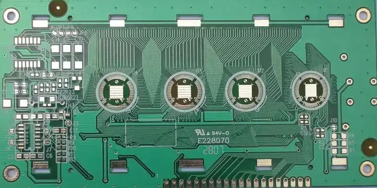
In the fast-evolving world of electronics, creating compact, high-performance printed circuit boards (PCBs) is more important than ever. If you're looking to maximize density in your PCB designs, Via-in-Pad (VIP) technology, combined with blind and buried vias, offers a powerful solution. This approach not only saves space but also improves thermal management and supports complex Ball Grid Array (BGA) routing for high-density layouts. In this blog, we'll dive deep into how VIP technology works, its benefits, and how it integrates with blind and buried vias to push the boundaries of modern PCB design.
What Is Via-in-Pad Technology?
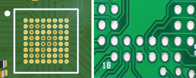
Via-in-Pad, often abbreviated as VIP, is a PCB design technique where a via—a small hole that connects different layers of a board—is placed directly under a component's pad. Traditionally, vias are positioned outside the pad area to avoid manufacturing issues like solder wicking. However, with VIP, the via is integrated into the pad itself, often filled and plated over to create a smooth surface for soldering.
This method is a game-changer for high-density PCB designs. By placing vias directly under components like BGAs, you free up valuable space on the board's surface. This allows for tighter component placement and more efficient routing, especially in compact devices like smartphones, wearables, and IoT gadgets. Additionally, VIP technology enhances thermal management by providing a direct path for heat dissipation from components to other layers or heat sinks.
Why Use Via-in-Pad in High-Density PCB Designs?
As electronic devices shrink in size, the demand for high-density interconnect (HDI) PCBs grows. VIP technology addresses several challenges in these designs, making it a preferred choice for engineers working on cutting-edge projects. Here are the key reasons to consider it:
- Space Optimization: With vias placed directly under component pads, you eliminate the need for additional routing space around pads. This can reduce board size by up to 30% in some designs, especially for fine-pitch BGAs with pin spacing as tight as 0.4mm.
- Improved Signal Integrity: Shorter connection paths reduce inductance and resistance, which is critical for high-speed signals. For example, VIP can lower loop inductance by approximately 50% compared to traditional via placements, ensuring cleaner signal transmission at speeds above 10 Gbps.
- Better Thermal Management: VIP creates a direct thermal path from heat-generating components to inner layers or heat sinks. This can reduce component temperatures by 10-15°C in high-power applications, extending device lifespan.
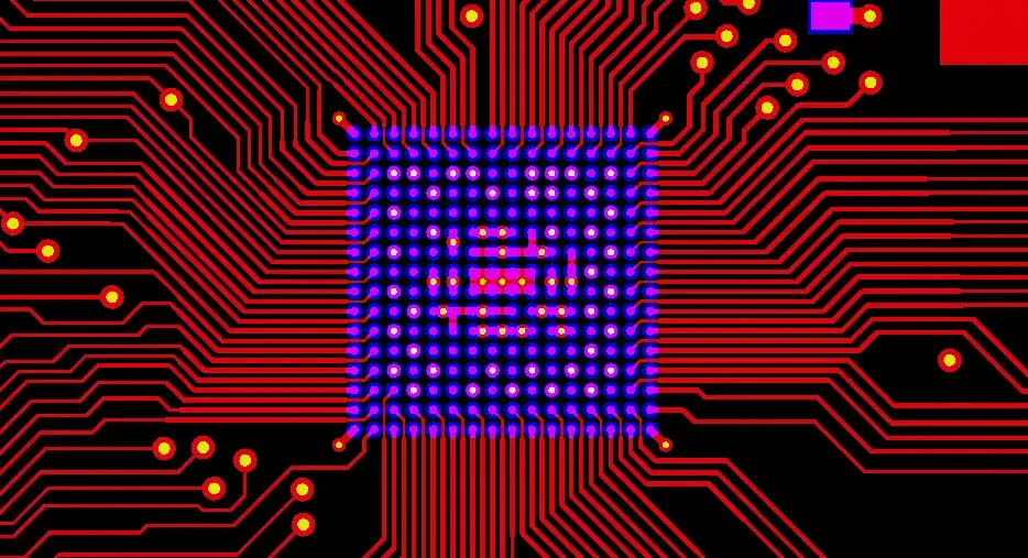
- Support for BGA Routing: BGAs often have hundreds or thousands of pins in a small area. VIP allows for efficient escape routing by placing vias directly under pins, avoiding cluttered surface traces.
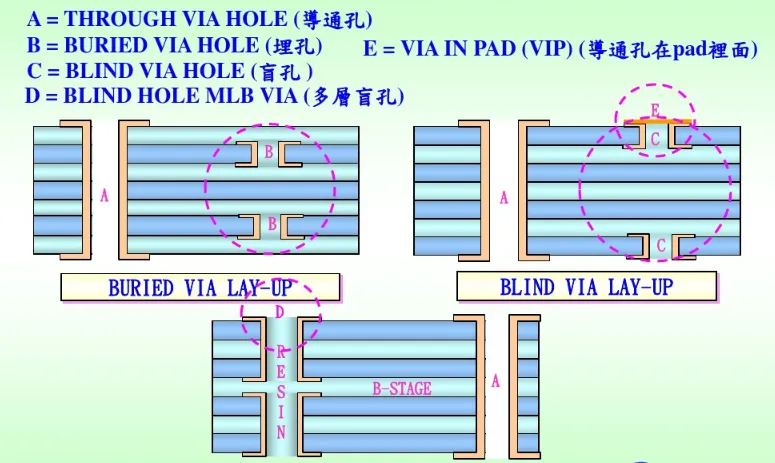
Understanding Blind and Buried Vias
To fully grasp how VIP technology maximizes density, it's essential to understand blind and buried vias, which often work hand-in-hand with VIP in HDI designs. These are specialized types of vias that don't span the entire thickness of the PCB, unlike traditional through-hole vias.
- Blind Vias: These connect an outer layer of the PCB to one or more inner layers but do not go through the entire board. For instance, a blind via might link layer 1 to layer 2 without reaching layer 6 in a six-layer board. This saves space on deeper layers and reduces signal interference.
- Buried Vias: These are located entirely within the internal layers of the PCB, connecting two or more inner layers without reaching the surface. For example, a buried via could connect layer 3 to layer 4 in a multi-layer board, leaving the outer layers free for other routing.
Both blind and buried vias are critical for high-density designs because they allow for more connections in a smaller area without cluttering the board's surface. When combined with VIP technology, they enable engineers to stack vias or create complex routing paths that would be impossible with standard through-hole vias.
How Via-in-Pad Works with Blind and Buried Vias
The synergy between VIP technology and blind or buried vias is what truly unlocks the potential of high-density PCB layouts. Here's how they complement each other:
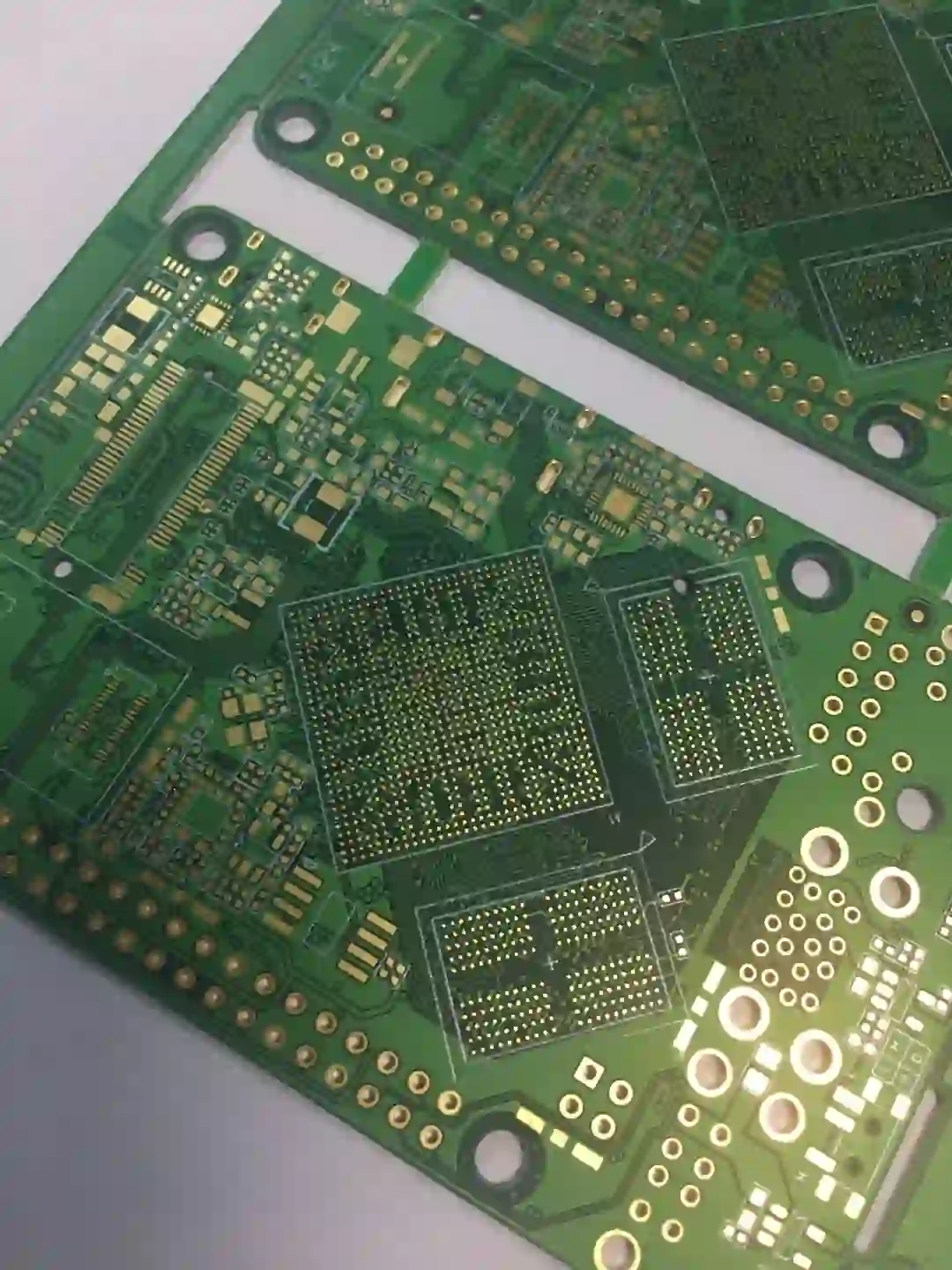
- Layer Optimization: Blind and buried vias free up space on outer layers by limiting via penetration. When paired with VIP, which places vias directly under pads, you can route signals to inner layers without wasting surface real estate. This is especially useful for BGAs with pin counts exceeding 1000, where surface space is at a premium.
- Reduced Crosstalk: By using buried vias to route signals internally, and VIP to shorten connection lengths, you minimize the risk of crosstalk in high-speed designs. This can improve signal integrity by reducing electromagnetic interference (EMI) by up to 20% in some cases.
- Enhanced Thermal Paths: VIP can be combined with thermal vias (a subset of blind or buried vias) to transfer heat from surface-mounted components to internal copper planes. This is vital for power-intensive chips, where heat dissipation can prevent thermal throttling.
For example, in a 12-layer PCB designed for a 5G module, VIP technology might be used under a BGA processor, with blind vias connecting the surface layer to layer 2 for power delivery, and buried vias routing high-speed signals between layers 4 and 6. This layered approach ensures a compact, efficient, and thermally stable design.
Benefits of Combining VIP with Blind and Buried Vias for BGA Routing
BGA components are widely used in modern electronics due to their high pin density and compact footprint. However, routing signals from a BGA with hundreds of pins can be a nightmare without the right techniques. Here's how VIP technology, combined with blind and buried vias, simplifies BGA routing in high-density PCBs:
- Escape Routing Made Easy: With VIP, vias are placed directly under BGA pins, allowing signals to escape to inner layers immediately. Blind vias can then route these signals to specific layers without interfering with other components on the surface.
- Reduced Trace Lengths: Shorter traces mean less signal delay and lower power loss. For high-speed BGAs operating at frequencies above 2 GHz, this can reduce signal latency by several picoseconds per trace.
- Support for Fine-Pitch BGAs: As BGA pitch shrinks to 0.5mm or less, traditional routing becomes nearly impossible. VIP combined with microvias (a type of blind via with diameters as small as 0.1mm) ensures reliable connections without increasing board size.
Thermal Management with Via-in-Pad Technology
Heat dissipation is a critical concern in high-density designs, where components are packed closely together, and power demands are high. VIP technology plays a significant role in thermal management by providing efficient heat transfer paths. Here's how it works:
- Direct Heat Paths: Vias placed under heat-generating components like processors or power ICs act as conduits, transferring heat to copper planes or heat sinks on other layers. This can lower junction temperatures by up to 20°C in some applications.
- Thermal Vias Integration: Thermal vias, often implemented as blind or buried vias, can be combined with VIP to create a grid of heat-dissipating structures under components. For instance, a 4x4 grid of thermal vias under a high-power chip can increase heat dissipation by 40% compared to a design without vias.
- Reduced Thermal Resistance: By minimizing the distance heat must travel, VIP reduces thermal resistance. This is especially important for designs with power densities exceeding 1 W/cm2, where overheating can degrade performance or cause failure.
Challenges and Considerations for Via-in-Pad Implementation
While VIP technology offers incredible benefits, it's not without challenges. Understanding these considerations ensures a successful implementation in your high-density PCB designs:
- Manufacturing Complexity: Placing vias under pads requires advanced fabrication techniques, such as via filling and plating over. This can increase production costs by 10-20% compared to standard PCB processes.
- Solder Wicking Risk: If not properly filled or capped, vias in pads can draw solder away from the component during assembly, leading to weak joints. Using conductive epoxy or copper filling mitigates this risk.
- Design Constraints: VIP often requires smaller via diameters (e.g., 0.2mm or less), which can limit current-carrying capacity. Engineers must balance via size with electrical and thermal needs.
To overcome these challenges, work closely with your fabrication partner to ensure they support VIP processes and can meet the required tolerances for your design.
Best Practices for Designing with Via-in-Pad and Blind/Buried Vias
To get the most out of VIP technology in your high-density PCB projects, follow these practical design tips:
- Optimize Via Size and Placement: Use the smallest via diameter possible (e.g., 0.1-0.2mm for microvias) to save space, but ensure it meets current and thermal requirements. Place VIPs under high-pin-count components like BGAs for maximum density.
- Use Layer Stacking Strategically: Plan your layer stack to incorporate blind and buried vias where surface space is limited. For example, route high-speed signals on inner layers using buried vias to reduce EMI.
- Prioritize Thermal Vias: For heat-intensive designs, include a grid of thermal vias under power components, connected to large copper planes for heat spreading.
- Simulate Signal Integrity: Use simulation tools to analyze signal performance with VIP and blind/buried vias. Ensure impedance matches your design specs, typically 50 ohms for high-speed lines.
Conclusion: The Future of High-Density PCB Design with VIP Technology
Via-in-Pad technology, when combined with blind and buried vias, is revolutionizing the way engineers approach high-density PCB design. By maximizing space, enhancing thermal management, and supporting complex BGA routing, this powerful combination enables the creation of smaller, faster, and more reliable electronic devices. Whether you're designing for 5G, IoT, or consumer electronics, integrating VIP into your workflow can give you a competitive edge.
As PCB technology continues to advance, staying ahead means adopting techniques like VIP to meet the demands of modern applications. With careful design and collaboration with manufacturing experts, you can overcome the challenges and unlock the full potential of high-density layouts for your next project.


