 ALLPCB


If you’re looking to understand the thick PCB manufacturing process, from prototyping to full-scale production, you’ve come to the right place. Thick PCBs, often used in high-power and industrial applications, require specialized techniques for fabrication and assembly due to their unique thickness and material properties. In this guide, we’ll walk you through every step of thick PCB prototyping, thick PCB fabrication, and thick PCB assembly, while addressing the challenges in thick PCB manufacturing. Whether you’re an engineer, designer, or project manager, this blog will provide actionable insights to help you succeed in your next project.
What Are Thick PCBs and Why Are They Important?
Thick PCBs are printed circuit boards with a greater thickness than standard boards, typically ranging from 2.0mm to 6.0mm or more, compared to the standard 1.6mm. These boards are designed to handle higher currents, provide better heat dissipation, and offer enhanced mechanical strength. They are commonly used in industries like automotive, aerospace, power electronics, and telecommunications, where durability and performance under stress are critical.
The importance of thick PCBs lies in their ability to support heavy copper layers (often 3 oz or more per square foot) and withstand harsh environments. For instance, in power supply systems, thick PCBs can manage high voltages and currents without overheating, ensuring reliable operation. Understanding the thick PCB manufacturing process is key to leveraging these benefits for your applications.
Step 1: Thick PCB Prototyping – Laying the Foundation
The journey of manufacturing thick PCBs begins with thick PCB prototyping. This stage is crucial for testing designs, identifying potential issues, and ensuring the board meets performance requirements before moving to mass production.
During prototyping, engineers create a small batch of boards using design files (often in Gerber format) to simulate the final product. The process starts with selecting the right materials, such as high-Tg FR-4 or specialized substrates for thermal management. For thick PCBs, material selection is even more critical due to the increased thickness and weight, which can affect signal integrity and heat dissipation.
A typical prototype for a thick PCB might have a thickness of 3.2mm and include 4-6 layers. Designers often test for impedance control, ensuring values stay within a tight tolerance (e.g., ±10% of 50 ohms for high-speed signals). Prototyping also involves checking for proper via drilling and plating, as thicker boards require deeper holes that can be challenging to fill uniformly.
One key tip during this phase is to collaborate closely with your manufacturing partner to validate the design for manufacturability (DFM). This helps catch errors early, such as insufficient spacing for heavy copper traces or potential warping due to uneven material distribution.
Step 2: Thick PCB Fabrication – Building the Core
Once the prototype is approved, the next step is thick PCB fabrication. This process involves multiple stages to create the physical board with precision and durability. Let’s break it down:
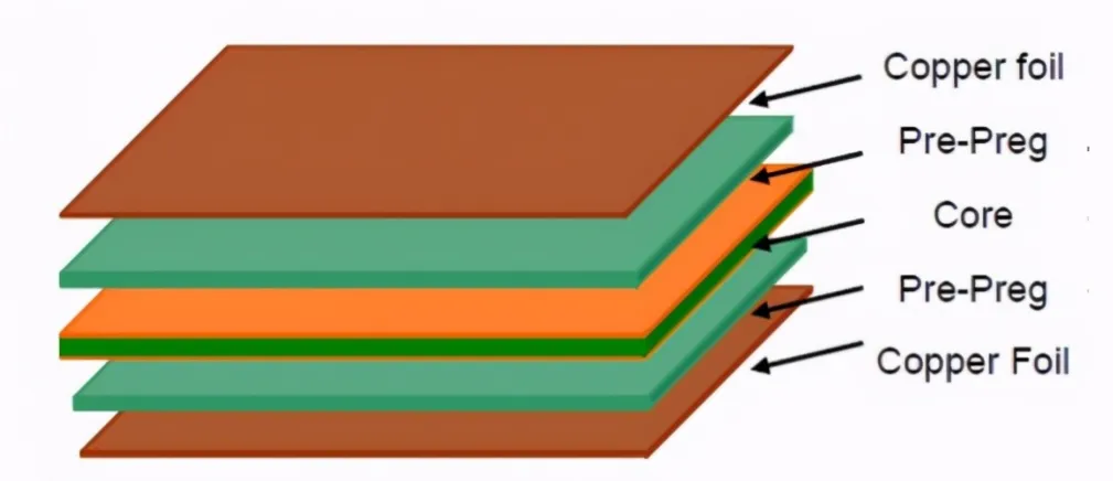
Material Preparation and Layer Stacking
The fabrication process begins with preparing the core materials. For thick PCBs, manufacturers often use multiple prepreg layers and copper foils to achieve the desired thickness. These layers are stacked and bonded under high pressure and temperature in a lamination process. A typical 4.0mm thick PCB might use 8-10 layers of material to ensure structural integrity.
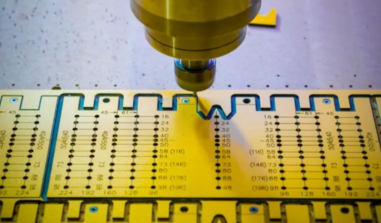
Drilling and Via Formation
Drilling is a critical step, especially for thick PCBs, as the increased depth requires specialized equipment to maintain accuracy. For example, a via in a 3.2mm board might need a depth-to-diameter ratio (aspect ratio) of 10:1 or higher, which demands precise control to avoid defects like incomplete plating or barrel cracks.
Copper Plating and Etching
After drilling, the board undergoes copper plating to create conductive paths through vias and on the surface. Thick PCBs often require heavier copper (e.g., 4 oz or 140 microns thick) to handle high currents, which can complicate the etching process. Uniform etching is essential to prevent undercutting or over-etching, which could weaken traces.
Surface Finishing
The final step in fabrication is applying a surface finish, such as ENIG (Electroless Nickel Immersion Gold) or HASL (Hot Air Solder Leveling), to protect the copper and ensure solderability. For thick PCBs used in high-power applications, a robust finish is vital to withstand thermal cycling and environmental stress.
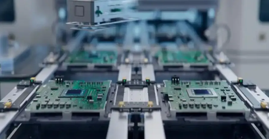
Step 3: Thick PCB Assembly – Bringing It All Together
After fabrication, the focus shifts to thick PCB assembly, where components are mounted onto the board. This stage presents unique challenges due to the board’s thickness and the high-power components often used.
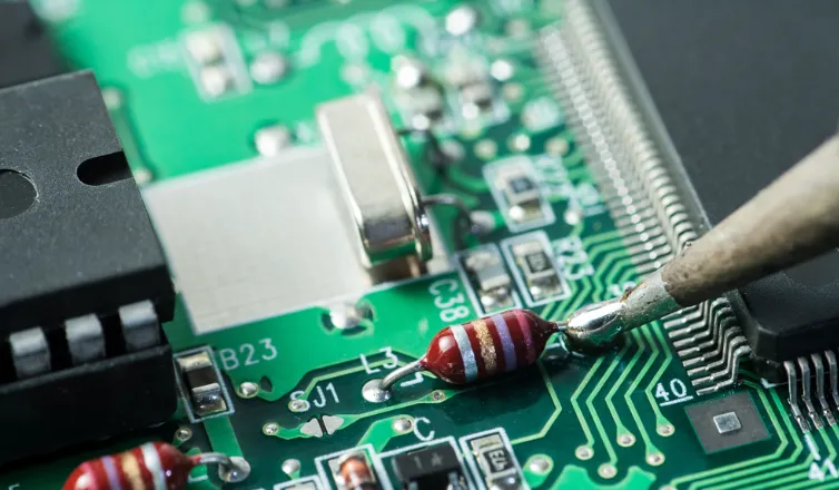
Surface Mount Technology (SMT) and Through-Hole Assembly
Thick PCBs often combine surface mount and through-hole components. SMT assembly requires precise placement of small components, while through-hole parts (common in power electronics) need robust soldering to handle the board’s weight and thermal load. For instance, a thick PCB for a motor controller might include large capacitors and connectors soldered via through-hole technology to ensure mechanical stability.
Thermal Management During Soldering
One major consideration during assembly is heat distribution. Thick PCBs absorb more heat during soldering, which can lead to uneven temperatures across the board. Manufacturers often use specialized reflow ovens with extended preheat zones to ensure consistent soldering without damaging components. For example, maintaining a peak temperature of 245°C for lead-free solder is critical to avoid cold joints or thermal shock.
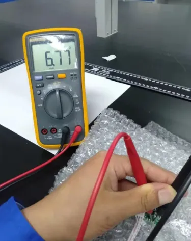
Inspection and Testing
Post-assembly, the board undergoes rigorous testing, including Automated Optical Inspection (AOI) and In-Circuit Testing (ICT), to verify solder joints and component placement. For thick PCBs, additional tests for thermal performance and current-carrying capacity are often conducted to ensure reliability under load.
Challenges in Thick PCB Manufacturing
While thick PCBs offer numerous advantages, there are significant challenges in thick PCB manufacturing that engineers and manufacturers must overcome. Addressing these challenges early can save time and cost in the long run.
Material and Structural Issues
Thicker boards are prone to warping or delamination during lamination due to uneven stress distribution. Using high-quality materials with consistent thermal expansion properties (e.g., a CTE of 14-16 ppm/°C) can mitigate this risk. Additionally, the increased weight of thick PCBs can complicate handling and assembly processes.
Drilling and Plating Difficulties
As mentioned earlier, drilling deep vias in thick PCBs requires high precision to maintain an acceptable aspect ratio. Poor plating in these vias can lead to weak connections or signal loss, especially in high-frequency applications where signal speeds might exceed 5 GHz.
Thermal and Electrical Challenges
Thick PCBs often operate in high-power environments, generating significant heat. Without proper thermal vias or heat sinks, temperatures can rise beyond safe limits (e.g., exceeding 125°C), risking component failure. Similarly, maintaining signal integrity for high-speed designs on thick boards requires careful impedance matching and layer planning.
Cost and Lead Time
Manufacturing thick PCBs is generally more expensive due to the specialized materials, equipment, and processes involved. Lead times can also be longer, especially for prototypes requiring multiple iterations to perfect the design. Planning ahead and optimizing the design for manufacturability can help manage these constraints.
Best Practices for Successful Thick PCB Projects
To navigate the complexities of thick PCB manufacturing, consider these best practices:
- Design with Manufacturing in Mind: Follow DFM guidelines to ensure your design is compatible with fabrication and assembly processes. For example, avoid placing vias too close to heavy copper areas to prevent plating issues.
- Choose the Right Materials: Select substrates and copper weights that match your application’s thermal and electrical needs. For high-power designs, consider using materials with a thermal conductivity of at least 1.0 W/m·K.
- Test Thoroughly During Prototyping: Use thick PCB prototyping to validate signal integrity, thermal performance, and mechanical strength before scaling to production.
- Partner with Experienced Manufacturers: Work with a manufacturing team that has expertise in thick PCBs to minimize errors and optimize production timelines.
From Prototype to Production – Scaling Up
Transitioning from prototype to full-scale production requires careful planning. Start by refining your design based on prototype feedback, ensuring all issues like signal loss or thermal hotspots are resolved. Next, finalize your Bill of Materials (BOM) and confirm component availability for large-scale assembly. Finally, conduct a pilot run to validate the production process before committing to a full batch.
During production, maintain close communication with your manufacturing partner to address any unforeseen challenges. Regularly review quality control data, such as defect rates or test pass percentages, to ensure consistency. For thick PCBs, a defect rate below 1% is often the target for high-reliability applications.
Conclusion: Mastering Thick PCB Manufacturing
Manufacturing thick PCBs, from thick PCB prototyping to production, is a complex but rewarding process. By understanding the intricacies of thick PCB fabrication and thick PCB assembly, and by addressing the challenges in thick PCB manufacturing, you can create robust, high-performance boards for demanding applications. Whether you’re designing for power electronics or industrial systems, following the steps and best practices outlined in this guide will help ensure success.
At ALLPCB, we’re committed to supporting your journey with expertise and cutting-edge solutions for thick PCB projects. With a focus on quality and precision, we’re here to help you bring your designs to life, from initial concept to final product.


