ALLPCB


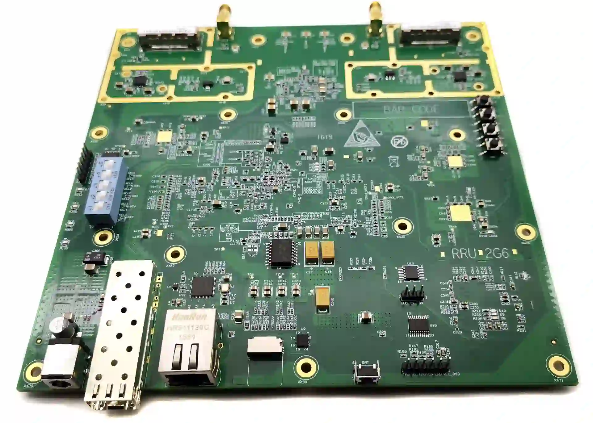
In the fast-paced world of telecommunications, ensuring signal integrity in base station PCBs (Printed Circuit Boards) is critical for reliable performance. Whether you're designing for 5G networks or other high-speed applications, maintaining clear and undistorted signals is a top priority. This guide dives deep into PCB signal integrity, offering practical solutions for base station PCB design rules, high-speed signal routing, impedance control PCB techniques, and crosstalk reduction techniques. Let’s explore how to optimize your designs for peak performance and minimal interference.
Why Signal Integrity Matters in Telecommunication Base Stations
Telecommunication base stations are the backbone of modern wireless networks, handling massive data transfers at lightning speeds. With frequencies often exceeding 1 GHz in 5G systems, even small signal distortions can lead to data loss, delays, or system failures. Poor signal integrity can result in dropped calls, slow internet speeds, or unreliable connections—issues no engineer wants to face.
Signal integrity refers to the ability of a signal to maintain its quality as it travels through a PCB. Factors like noise, crosstalk, and impedance mismatches can degrade signals, especially in high-speed designs. By focusing on robust design practices, you can ensure that your base station PCBs deliver consistent, high-quality performance.
Key Challenges in Base Station PCB Design
Designing PCBs for base stations comes with unique challenges due to the high-frequency signals and complex layouts involved. Some of the main hurdles include:
- High-Speed Signals: Data rates in modern systems can reach 10 Gbps or higher, increasing the risk of signal degradation.
- Electromagnetic Interference (EMI): External and internal noise can disrupt signals, especially in dense urban environments.
- Compact Layouts: Base station equipment often requires tightly packed components, making routing and interference management tricky.
- Thermal Management: High-speed circuits generate heat, which can affect signal stability if not addressed.
Overcoming these challenges requires a solid understanding of base station PCB design rules and targeted strategies to protect signal integrity.
Essential Base Station PCB Design Rules for Signal Integrity
Following proven design rules is the foundation of maintaining signal integrity in telecommunication base station PCBs. Here are key guidelines to implement:
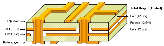
1. Prioritize Layer Stack-Up Design
A well-planned layer stack-up is crucial for controlling signal paths and minimizing interference. For high-speed designs, use a multilayer PCB with dedicated ground and power planes. A typical stack-up for a base station PCB might include:
- Top layer for signal traces
- Ground plane to provide a stable reference
- Power plane for clean voltage distribution
- Additional signal layers with ground planes in between
Ground planes act as a shield, reducing EMI and providing a low-impedance return path for signals. Ensure that ground planes are continuous under high-speed signal traces to avoid disruptions.
2. Control Trace Width and Spacing
Trace width and spacing directly impact signal integrity. For high-frequency signals, traces should be designed to maintain a specific impedance, often 50 ohms for RF applications. Use trace width calculators to determine the correct dimensions based on your PCB material and layer thickness. As a general rule, maintain at least 3 times the trace width as spacing between adjacent high-speed traces to minimize crosstalk.
3. Minimize Via Usage
Vias introduce inductance and capacitance, which can distort high-speed signals. When vias are necessary, use blind or buried vias to reduce stub lengths, and avoid placing vias in critical signal paths. For example, in a 5G base station design operating at 3.5 GHz, excessive vias can cause signal reflections, leading to a loss of up to 10% in signal strength.
High-Speed Signal Routing Strategies
Routing high-speed signals in base station PCBs requires precision to avoid delays, reflections, and interference. Let’s dive into actionable high-speed signal routing techniques:
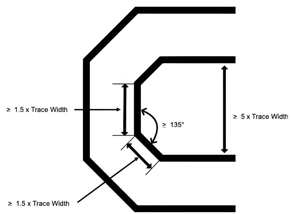
1. Keep Traces Short and Direct
Longer traces increase the chance of signal loss and delay. Route high-speed signals as straight as possible, avoiding sharp bends. If bends are needed, use 45-degree angles instead of 90-degree turns to reduce signal reflections. For instance, in a design handling 10 Gbps data, a trace length difference of just 1 inch can introduce a timing skew of about 150 picoseconds.
2. Use Differential Pair Routing
For high-speed data like Ethernet or PCIe in base stations, differential pairs are common. These pairs carry complementary signals, canceling out noise when routed closely together. Maintain equal trace lengths for both lines in the pair, and keep spacing consistent to ensure balanced impedance. A mismatch of even 5 mils can cause signal skew, degrading performance.
3. Avoid Routing Over Splits
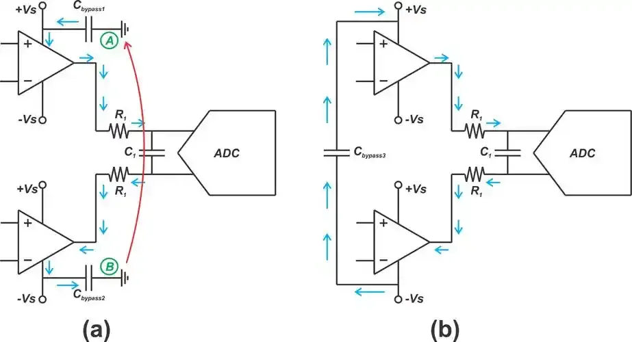
Never route high-speed signals over splits in ground or power planes. A split disrupts the return path, causing EMI and signal distortion. If a split is unavoidable, place stitching capacitors near the crossing to provide a return path for the signal.
Impedance Control in PCB Design
One of the cornerstones of signal integrity is impedance control PCB design. Impedance mismatches cause signal reflections, leading to data errors and reduced performance. Here’s how to manage impedance effectively:
1. Understand Characteristic Impedance
Characteristic impedance is the resistance a signal encounters as it travels along a trace. For most high-speed designs in telecommunication, a 50-ohm impedance is standard. Use PCB design software to calculate the required trace width and dielectric thickness based on your board’s material (e.g., FR-4 with a dielectric constant of 4.2).
2. Match Impedance at Terminations
Ensure that the source, trace, and load impedances are matched. For example, if a transmitter outputs a 50-ohm signal, the trace and receiver should also be 50 ohms. Mismatches can reflect up to 20% of the signal energy back to the source, causing interference.
3. Test and Validate Impedance
After fabrication, use a Time Domain Reflectometer (TDR) to measure the impedance of critical traces. If deviations are found, adjust your design parameters or work with your PCB manufacturer to refine the process. Consistent impedance across a board can improve signal quality by up to 15% in high-speed applications.
Crosstalk Reduction Techniques for Base Station PCBs
Crosstalk occurs when signals from one trace interfere with another, a common issue in densely packed base station designs. Implementing crosstalk reduction techniques is essential for clean signal transmission:
1. Increase Trace Spacing
The simplest way to reduce crosstalk is to increase the spacing between traces. A spacing of 3 times the trace width (often called the 3W rule) can reduce crosstalk by up to 70%. For critical signals, consider even larger spacing or routing on different layers.
2. Use Guard Traces
Place grounded guard traces between high-speed signal lines to act as a barrier against interference. Connect these traces to the ground plane with vias at regular intervals (e.g., every 0.5 inches) to maintain a low-impedance path.
3. Leverage Solid Ground Planes
A solid, unbroken ground plane under signal traces provides a stable reference and reduces crosstalk. Avoid routing signals on layers without a nearby ground plane, as this can increase interference by up to 50% in high-frequency designs.
Advanced Tips for Optimizing Signal Integrity
Beyond the basics, here are some advanced strategies to further enhance PCB signal integrity in base station designs:
1. Simulate Before Fabrication
Use simulation tools to model signal behavior under different conditions. Tools can predict issues like crosstalk, reflections, and EMI before you build the board, saving time and cost. For instance, simulating a 5G base station PCB at 3.5 GHz can reveal potential signal loss areas with 95% accuracy.
2. Choose the Right Materials
Standard FR-4 materials may not suffice for ultra-high-frequency designs. Consider low-loss materials like Rogers or Isola, which offer dielectric constants as low as 3.0, reducing signal loss by up to 30% at frequencies above 5 GHz.
3. Implement Decoupling Capacitors
Place decoupling capacitors close to power pins of high-speed components to filter noise. Use a mix of capacitance values (e.g., 0.1 μF and 1 μF) to cover a wide frequency range, ensuring stable power delivery to critical circuits.
Conclusion: Building Reliable Base Station PCBs
Maximizing signal integrity in telecommunication base station PCBs is a complex but achievable goal. By adhering to base station PCB design rules, optimizing high-speed signal routing, ensuring impedance control PCB practices, and applying effective crosstalk reduction techniques, you can create designs that perform reliably under demanding conditions. Focus on precise planning, simulation, and material selection to tackle the unique challenges of high-frequency applications.
With the right approach, your base station PCBs will support the next generation of wireless communication, delivering fast, clear, and uninterrupted signals. Start implementing these strategies in your next project to see the difference in performance and reliability.