 ALLPCB


In the world of PCB design, understanding the concepts of creepage and clearance is essential for creating safe and reliable electronic products. For electronics engineers, the difference between creepage vs clearance in PCB design can mean the difference between a successful project and a catastrophic failure. This guide will break down these critical concepts, provide a clearance and creepage distance table, explain creepage distance measurement, and outline PCB design rules for creepage to help you design with confidence.
Whether you're working on high-voltage systems or compact circuit boards, mastering these principles ensures safety and compliance with industry standards. Let’s dive into the details of creepage and clearance, offering practical insights and actionable tips for your next project.
What Are Creepage and Clearance in PCB Design?
Before we explore the specifics, let’s define creepage and clearance in simple terms. These two measurements are crucial for maintaining electrical safety in PCB layouts by preventing unintended electrical discharges or breakdowns.
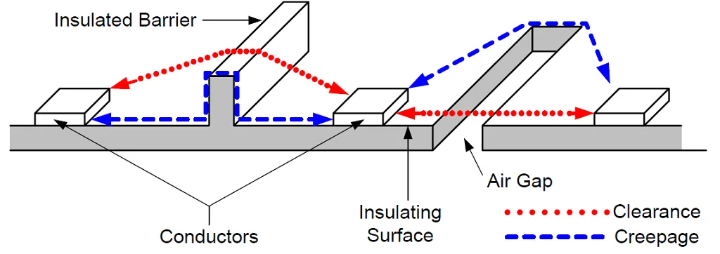
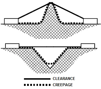
- Clearance: This is the shortest distance between two conductive parts through the air. It’s the direct "line of sight" path that an electrical arc could take if the voltage is high enough to jump the gap.
- Creepage: This refers to the shortest distance between two conductive parts along the surface of an insulating material. It accounts for the path that electricity might "creep" along due to contamination, dust, or moisture on the board's surface.
Understanding creepage vs clearance in PCB design is vital because each serves a different purpose in preventing electrical failures. Clearance protects against arcing through the air, while creepage guards against surface tracking. Both are influenced by factors like voltage levels, environmental conditions, and the materials used in your PCB.
Why Creepage and Clearance Matter in PCB Design
In high-voltage applications, insufficient creepage or clearance can lead to electrical arcing, short circuits, or even fires. For electronics engineers, adhering to proper spacing rules isn’t just about functionality—it’s about safety and compliance with international standards like IEC 60950 or IPC-2221.
Even in low-voltage designs, neglecting these distances can cause issues, especially in environments with high humidity or pollution. For instance, a PCB in an industrial setting might accumulate dust, reducing the effective creepage distance and increasing the risk of failure. By prioritizing these measurements, you ensure your design withstands real-world conditions and meets regulatory requirements.
Key Factors Influencing Creepage and Clearance Distances
Several factors determine the required creepage and clearance distances for a PCB. Understanding these will help you apply the right PCB design rules for creepage and clearance in your projects.
- Working Voltage: Higher voltages require larger distances to prevent arcing. For example, a 500V system may need a clearance of 4mm or more, depending on the standard.
- Pollution Degree: This refers to the level of contamination in the operating environment. A pollution degree of 3 (industrial settings with high dust or moisture) demands greater creepage distances than a pollution degree of 1 (clean, controlled environments).
- Material Properties (CTI): The Comparative Tracking Index (CTI) of the PCB material affects creepage. Materials with a lower CTI are more prone to surface tracking and require larger distances.
- Altitude: At higher altitudes, air pressure decreases, reducing the dielectric strength of air. This means clearance distances must be increased for designs operating above 2000 meters.
- Insulation Type: The type of insulation (functional, basic, or reinforced) impacts the required distances. Reinforced insulation, used in safety-critical applications, often demands double the distance of basic insulation.
By factoring in these elements, you can tailor your design to meet specific safety and performance needs.
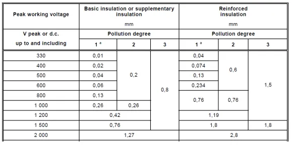
Clearance and Creepage Distance Table for PCB Design
To make things practical, below is a simplified clearance and creepage distance table based on common industry standards like IPC-2221. Note that these values are general guidelines for low to medium voltage designs and may vary based on specific standards, pollution degrees, or applications. Always consult the relevant standard for your project.
| Voltage (Peak or DC) | Clearance (mm) | Creepage (mm) - Pollution Degree 2 |
|---|---|---|
| 0-50V | 0.6 | 0.9 |
| 51-100V | 0.6 | 1.2 |
| 101-150V | 0.8 | 1.6 |
| 151-300V | 1.6 | 3.2 |
| 301-500V | 3.2 | 6.0 |
This table provides a starting point for typical designs, but for high-voltage or safety-critical applications, additional margins or specific standards may apply. For instance, medical devices often require stricter distances due to reinforced insulation needs.
How to Measure Creepage Distance on a PCB
Creepage distance measurement is a critical step in validating your PCB design. Unlike clearance, which is a straight-line measurement through air, creepage follows the surface of the insulating material, making it trickier to calculate. Here’s how to do it effectively:
- Identify Conductive Parts: Locate the two conductive elements (e.g., traces, pads, or components) between which you’re measuring the creepage distance.
- Trace the Surface Path: Determine the shortest path along the surface of the PCB material between these parts. This path may go around slots, grooves, or barriers if they are present.
- Account for Barriers: If your design includes slots or insulating barriers to increase creepage distance, include only the effective path around these features. For example, a 1mm-wide slot can significantly extend the creepage path.
- Use Design Tools: Many PCB design software tools have built-in features to calculate creepage and clearance automatically. Use these to verify manual measurements.
For instance, if two traces are separated by a 2mm straight-line distance but a slot in the PCB forces the surface path to be 5mm, the creepage distance is 5mm. Accurate measurement ensures your design meets safety standards and prevents surface tracking.
PCB Design Rules for Creepage and Clearance
Following PCB design rules for creepage and clearance is non-negotiable for creating safe and reliable boards. Below are practical guidelines to integrate into your workflow:
1. Plan Spacing Early in the Design Process
Don’t leave creepage and clearance as an afterthought. During the schematic and layout phases, allocate sufficient space for high-voltage areas. For a 300V circuit, ensure at least 3.2mm clearance and 6mm creepage (as per the table above) between critical traces.
2. Use Slots and Barriers
In compact designs where space is limited, slots or grooves in the PCB can increase creepage distance without enlarging the board. A slot of just 0.5mm width can double the effective creepage path in tight layouts.
3. Choose the Right Materials
Select PCB materials with a high CTI value (e.g., FR-4 with CTI > 175) to reduce the required creepage distance. This is especially important for boards in harsh environments.
4. Separate High and Low Voltage Areas
Group high-voltage components and traces away from low-voltage sections. Use physical barriers or separate layers if needed to maintain safe distances.
5. Test and Validate
After completing your layout, use design rule checks (DRC) in your PCB software to verify creepage and clearance distances. Additionally, perform physical testing under simulated environmental conditions (e.g., high humidity) to ensure reliability.
By adhering to these PCB design rules for creepage, you minimize risks and enhance the longevity of your product.
Common Challenges and Solutions in Creepage and Clearance Design
Even with the best planning, engineers often face challenges in meeting creepage and clearance requirements. Here are some common issues and how to address them:
- Limited Board Space: In compact designs, fitting components while maintaining distances is tough. Solution: Use multilayer boards to separate high-voltage traces vertically, or incorporate insulating barriers.
- High Pollution Environments: Dust and moisture can reduce effective creepage. Solution: Apply conformal coating to protect the PCB surface and increase creepage resistance.
- Complex Standards: Navigating multiple standards (e.g., IEC vs. IPC) can be confusing. Solution: Identify the primary standard for your industry early on and use software tools to automate compliance checks.
Addressing these challenges proactively saves time and reduces the risk of costly redesigns.
Tools and Resources for Creepage and Clearance Compliance
Modern PCB design tools simplify the process of ensuring proper creepage and clearance. Many software platforms offer built-in calculators and rule-checking features to flag violations during the design phase. Additionally, online resources like creepage and clearance calculators can provide quick estimates based on voltage and environmental factors.
For standards and detailed guidelines, refer to documents like IPC-2221 (for general PCB design) or IEC 60601 (for medical devices). These resources provide comprehensive tables and formulas to calculate distances accurately for your specific application.
Conclusion: Building Safer PCBs with Creepage and Clearance Mastery
Mastering creepage and clearance in PCB design is a fundamental skill for electronics engineers. By understanding the nuances of creepage vs clearance in PCB layouts, using a clearance and creepage distance table, performing accurate creepage distance measurement, and following PCB design rules for creepage, you can create boards that are both safe and reliable.
Remember to consider factors like voltage, pollution degree, and material properties when planning your layout. Use design tools to validate your work and stay updated on industry standards to ensure compliance. With these practices, you’ll be well-equipped to tackle high-voltage designs and deliver exceptional results in your projects.
Start applying these principles in your next PCB design to enhance safety and performance. Your attention to detail in creepage and clearance will set your work apart in the field of electronics engineering.


