 ALLPCB


Are you looking to optimize your PCB design with an asymmetrical stackup for better performance? An asymmetrical stackup can be a powerful tool for PCB designers, offering flexibility to meet specific design needs like impedance control, crosstalk reduction, and EMI mitigation. In this comprehensive guide, we’ll walk you through the essentials of asymmetrical stackup design, providing actionable tips and insights tailored for PCB engineers. Whether you're searching for an asymmetrical stackup tutorial or PCB design tips, this post will help you master the art of creating high-performing boards with a focus on impedance control, crosstalk, and EMI reduction.
What Is an Asymmetrical Stackup in PCB Design?
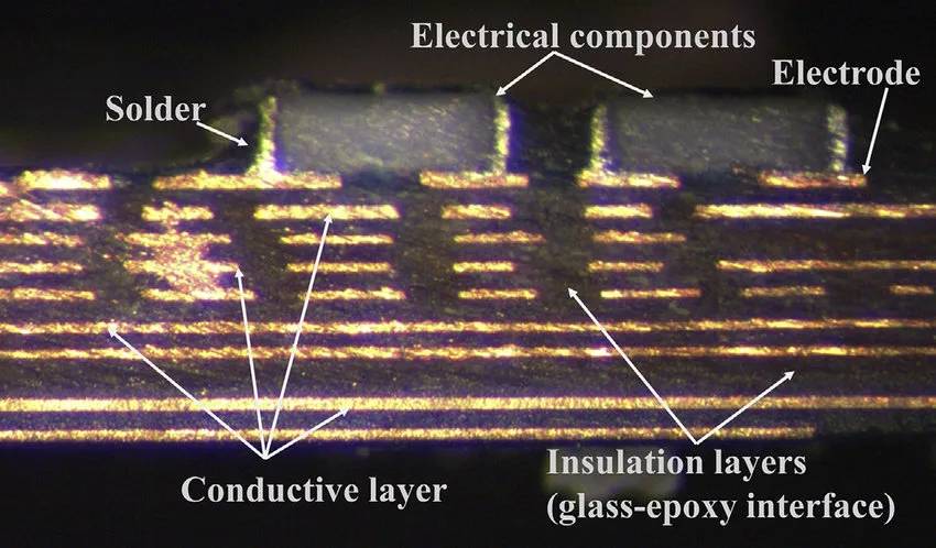
In PCB design, a stackup refers to the arrangement of conductive and insulating layers in a multilayer board. Most traditional designs use a symmetrical stackup, where layers are mirrored around the center for balance. However, an asymmetrical stackup breaks this balance by having an uneven distribution of layers or materials on either side of the board’s core. This approach can be intentional, allowing designers to address specific electrical or mechanical requirements.
For instance, an asymmetrical stackup might place more signal layers on one side of the board to optimize routing for high-speed signals, or it could use different dielectric materials to control impedance in critical areas. While this design can introduce challenges like warping during manufacturing, it offers unique benefits for advanced applications. Let’s dive deeper into why and how to use asymmetrical stackups effectively.
Why Choose an Asymmetrical Stackup? Benefits for PCB Designers
Asymmetrical stackups are not the default choice for most designs, but they shine in specific scenarios. Here are some key reasons to consider this approach:
- Optimized Impedance Control: By adjusting layer thickness and material properties on one side of the board, you can fine-tune impedance for high-speed signals. For example, a thinner dielectric on the top layers can help achieve a 50-ohm impedance for critical traces.
- Reduced Crosstalk: Strategic placement of ground planes closer to signal layers on one side can minimize crosstalk between adjacent traces, especially in dense designs.
- EMI Reduction: Asymmetrical designs allow for better placement of shielding layers or ground planes near sensitive components, cutting down electromagnetic interference (EMI).
- Space Efficiency: If your design requires more routing on one side (e.g., for surface-mounted components), an asymmetrical stackup can provide the extra layers needed without increasing the overall board thickness unnecessarily.
While these benefits are compelling, asymmetrical stackups require careful planning to avoid issues like thermal imbalance or manufacturing defects. Let’s explore how to design one effectively.
Step-by-Step Asymmetrical Stackup Tutorial for PCB Designers
Creating an asymmetrical stackup that performs well involves several steps. Follow this practical guide to ensure your design meets electrical and mechanical goals.
Step 1: Define Your Design Requirements
Start by identifying the specific needs of your project. Are you prioritizing impedance control for high-speed signals? Do you need to reduce crosstalk between traces? Or is EMI reduction your primary concern? For example, if you’re designing a board for a 5G application, you might need tightly controlled impedance (e.g., 50 ohms) for RF signals, which could dictate a thinner dielectric on the top layers.
Step 2: Choose the Right Layer Configuration
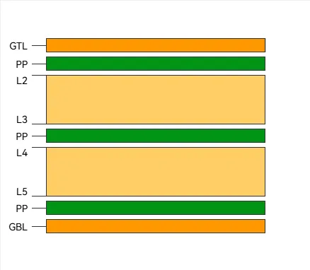
Unlike symmetrical stackups, where layers are balanced (e.g., a 4-layer board with two signal layers and two ground planes), an asymmetrical design might have three signal layers on one side and a single power plane on the other. A common 6-layer asymmetrical stackup could look like this:
- Layer 1: Signal (Top)
- Layer 2: Ground
- Layer 3: Signal
- Layer 4: Signal
- Layer 5: Power
- Layer 6: Ground (Bottom)
This configuration prioritizes signal routing on the top half while maintaining ground planes for shielding. Use simulation tools to validate your layer arrangement before finalizing it.
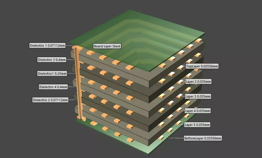
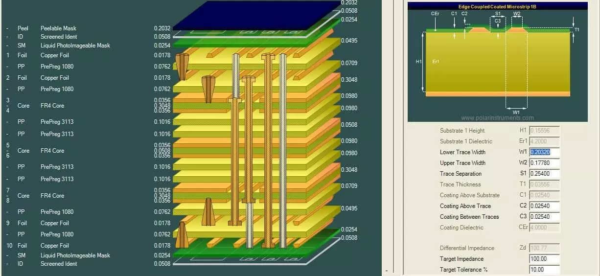
Step 3: Select Materials and Dielectric Thickness
Material selection plays a critical role in an asymmetrical stackup. Different dielectric thicknesses or materials (like FR-4 or high-frequency laminates) can be used on either side of the core to achieve desired electrical properties. For instance, a dielectric constant (Dk) of 3.5 on the top layers can support faster signal propagation compared to a Dk of 4.2 on the bottom layers. Be mindful of thermal expansion differences, as mismatched materials can lead to board warping.
Step 4: Simulate and Test for Impedance Control
Impedance mismatches can ruin signal integrity, especially in high-speed designs. Use a field solver or PCB design software to calculate the characteristic impedance of your traces. For a target of 50 ohms, you might need a trace width of 6 mils and a dielectric thickness of 4 mils on the top layer. Adjust the stackup if the simulation shows deviations beyond acceptable limits (e.g., ±10% tolerance).
Step 5: Address Manufacturing Challenges
Asymmetrical stackups are prone to warping due to uneven stress during lamination. Work closely with your fabrication partner to balance copper distribution and choose a core material that minimizes thermal mismatch. Some designers add dummy copper fills on less dense layers to even out the stress, though this must be done without affecting signal integrity.
PCB Design Tips for Asymmetrical Stackups
Beyond the basic steps, here are some practical PCB design tips to ensure your asymmetrical stackup performs as intended. These tips focus on impedance control, crosstalk, and EMI reduction—key concerns for modern electronics.
Tip 1: Prioritize Ground Plane Placement for Crosstalk Reduction
Crosstalk occurs when signals on adjacent traces interfere with each other, often due to electromagnetic coupling. In an asymmetrical stackup, place ground planes closer to high-speed signal layers to act as a shield. For example, if layers 1 and 3 carry high-frequency signals, ensure layer 2 is a solid ground plane with no splits. This can reduce crosstalk by up to 30% in some designs, based on typical industry simulations.
Tip 2: Use Differential Pairs for Better Impedance Control
For high-speed signals, route critical traces as differential pairs. This technique ensures consistent impedance (e.g., 100 ohms for differential lines) and reduces susceptibility to noise. In an asymmetrical stackup, keep the pair on the same layer and maintain equal trace lengths to avoid skew, which can degrade signal timing by nanoseconds.
Tip 3: Minimize EMI with Strategic Layering
Electromagnetic interference (EMI) can disrupt nearby circuits or fail compliance tests. In an asymmetrical design, place sensitive analog signals on layers furthest from noisy digital or power traces. Adding a ground plane near the top layer can also act as a shield, cutting EMI radiation by as much as 20 dB in certain frequency ranges, according to common design studies.
Tip 4: Balance Copper Distribution
Even in an asymmetrical stackup, strive for balanced copper density across layers to prevent manufacturing issues. If one side of the board has dense routing, use copper pours or dummy fills on the opposite side. Uneven copper can cause a bow or twist of up to 0.5% of the board’s diagonal length, per standard fabrication guidelines.
Common Challenges and How to Overcome Them
While asymmetrical stackups offer flexibility, they come with unique hurdles. Here’s how to tackle the most common issues:
- Thermal Imbalance: Different layer counts or materials can cause uneven heating, leading to warping. Mitigate this by using prepregs and cores with similar coefficients of thermal expansion (CTE), ideally within 10-15 ppm/°C of each other.
- Signal Integrity Risks: Asymmetrical designs can complicate return paths for signals. Ensure continuous ground planes beneath high-speed traces to provide a low-impedance return path, reducing signal delays or reflections.
- Manufacturing Costs: Custom stackups often increase fabrication costs due to specialized processes. Optimize your design early through simulations to avoid costly revisions, and communicate clearly with your manufacturer about tolerances.
Tools and Resources for Asymmetrical Stackup Design
Designing an asymmetrical stackup is easier with the right tools. Many PCB design platforms offer stackup editors and simulation features to test impedance and signal integrity. Look for software that includes:
- Layer stackup builders to visualize asymmetrical arrangements.
- Impedance calculators to predict trace behavior (e.g., achieving 50 ohms for single-ended signals).
- EMI and crosstalk analysis modules to identify potential issues before fabrication.
Additionally, collaborate with your fabrication partner for stackup recommendations tailored to their processes. Many provide free stackup design guides or calculators to ensure manufacturability.
Real-World Applications of Asymmetrical Stackups
Asymmetrical stackups are particularly useful in specialized fields. For example:
- RF and Microwave Designs: These often require precise impedance control (e.g., 50 ohms for RF lines) and minimal EMI, achievable with asymmetrical layering of high-frequency materials on one side.
- High-Speed Digital Boards: In applications like DDR4 memory interfaces, asymmetrical stackups help manage signal density and crosstalk for data rates exceeding 3.2 Gbps.
- Mixed-Signal Systems: Separating analog and digital signals on different sides of the board reduces interference, a common use case for asymmetrical designs.
Conclusion: Mastering Asymmetrical Stackups for Better PCB Performance
An asymmetrical stackup can be a game-changer for PCB designers tackling complex challenges like impedance control, crosstalk, and EMI reduction. By carefully planning your layer arrangement, selecting appropriate materials, and following best practices, you can harness the benefits of this unconventional approach without compromising on manufacturability or performance. Use the steps and PCB design tips in this asymmetrical stackup tutorial to create boards that meet the demands of modern electronics, from high-speed digital to sensitive RF applications.
With a focus on practical solutions and real-world insights, this guide equips you with the knowledge to experiment with asymmetrical stackups confidently. Start small, simulate often, and collaborate with your fabrication team to refine your designs. The result will be a PCB that not only meets but exceeds your project’s requirements.


