ALLPCB


In the intricate world of electronics, the printed circuit boards (PCBs) is evolving at a rapid pace. One of the most advanced types of PCBs is the 8-layer PCB, a marvel of modern engineering designed to meet the demands of high-performance and compact electronic devices. This blog post will guide you through the intricacies of 8-layer PCBs, shedding light on when and why they are used, the design considerations involved, their manufacturing process, and their applications. By the end of this article, you'll have a comprehensive understanding of 8-layer PCBs and how they can revolutionize your electronic projects.
What is 8 Layer PCB?
An 8-layer PCB is a type of multilayer printed circuit board that includes eight conductive copper layers separated by insulating material (prepreg and core). This structure allows for more complex and compact circuit designs, making it ideal for high-speed, high-density, and high-frequency applications.
The standard stackup typically includes:
-
4 signal layers
-
2 power planes
-
2 ground planes
Each layer serves a specific function, such as power delivery, signal routing, or shielding, contributing to superior performance and electromagnetic compatibility (EMC).
When and Why to Use 8-Layer PCBs
High-Density Interconnect (HDI) Applications
8-layer HDI PCBs are particularly useful in high-density interconnect (HDI) applications. When electronic devices require complex circuitry within a limited space, 8-layer PCBs offer the ideal solution. Their multiple layers allow for increased routing options, reducing the need for long and convoluted traces.
Enhanced Signal Integrity
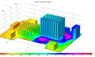
Signal integrity is a critical factor in high-speed electronic circuits. The additional layers in an 8-layer PCB help in separating signal layers with ground or power planes, minimizing crosstalk and electromagnetic interference (EMI). This results in more reliable signal transmission.
Efficient Power Distribution
For devices that consume significant power, managing power distribution efficiently is crucial. 8-layer PCBs provide additional layers for power planes, ensuring stable and efficient power delivery to various components.
Design of 8-Layer PCBs
Layer Stackup Configuration
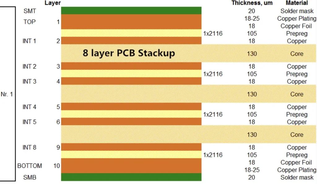
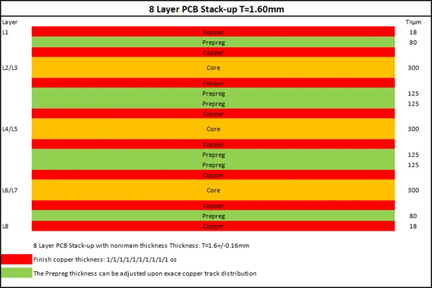
Designing an 8-layer PCB requires careful consideration of the layer stackup configuration. A typical 8-layer PCB might include layers designated for signals, ground planes, and power planes. Proper arrangement of these layers is essential to optimize performance and minimize EMI.
ALLPCB can recommend stackup structures according to the Board Thickness,
Inner Copper Thickness, and Outer Copper Thickness. You can check our 8-layer-laminated structure diagrams.
Routing Direction
In an 8-layer PCB, adjacent signal layers should be routed perpendicularly to each other to minimize crosstalk. This routing strategy helps in maintaining signal integrity, especially in high-speed circuits.
Return Path Management
High-speed signals require a clear and short return path to minimize interference. Ensuring that the return path does not overlap with other signal paths is crucial for maintaining signal integrity.
Ground Plane Considerations
A continuous ground plane is essential for reducing impedance discontinuities and providing a stable reference for signal layers. Splitting the ground plane can lead to performance issues, so it's best to keep it intact.
Suggested Reading: 8-Layer PCB Art: Designing Functional and Beautiful Circuit Boards
Manufacturing of 8-Layer PCBs
Material Selection
The choice of materials for the different layers in an 8-layer PCB significantly impacts its performance. Common materials include PCB material FR4 for the core and prepregs, but high-speed materials like Rogers or Isola may be used for specific applications requiring better signal integrity.
| Material Type | Features | Application Focus |
|---|---|---|
| FR-4 (Standard) | Low cost, good mechanical strength | Consumer electronics |
| High-Tg FR-4 | High temperature resistance | Automotive, industrial |
| Polyimide | Excellent thermal stability | Aerospace, military |
| Rogers/Isola/Arlon | Low dielectric loss for high-frequency signal | RF, 5G, radar |
Read more: 8-Layer PCB Stackup: Choosing the Right Materials for Your Application
Layer Alignment and Bonding
During manufacturing, precise alignment of the layers is critical to ensure the functionality of the PCB. The layers are bonded together using heat and pressure, creating a unified structure.
Etching and Plating
The conductive layers are etched to create the desired circuit patterns, and holes are drilled and plated to create vias that connect the different layers. These processes require high precision to maintain the integrity of the design.
Quality Control and Testing
Rigorous quality control measures are employed to ensure the reliability of 8-layer PCBs. These include visual inspections, electrical testing, and thermal analysis to detect any defects or performance issues.

Applications of 8-Layer PCBs
Telecommunications
In telecommunications equipment, 8-layer PCBs are used to manage complex signal routing and power distribution, ensuring reliable communication.
Aerospace and Defense
Aerospace and defense systems require high-performance, reliable PCBs. 8-layer PCBs provide the necessary complexity and robustness to meet these demands.
Read more: 8-Layer PCB Design for Aerospace Applications: Meeting Stringent Requirements
Power Electronics
Used in electric vehicle control systems, power inverters, industrial drives, and high-efficiency power supplies, 8-layer PCBs can support high current loads while maintaining thermal performance. The dedicated power and ground planes facilitate optimal current return paths.
Read more: 8-Layer PCB for Power Electronics: Handling High Current and Voltage
Automotive Industry
In modern vehicles, electronic systems control everything from infotainment to advanced driver-assistance systems (ADAS). 8-layer PCBs are integral in managing these complex electronic circuits.
Internet of Things (IoT) Devices
IoT hardware, including smart sensors, wearable devices, and home automation controllers, demands compact, energy-efficient designs that can manage wireless protocols like Wi-Fi, Bluetooth, and Zigbee. The added layers in 8-layer PCBs support complex routing and minimize cross-talk in tight layouts.
Read more: 8-Layer PCB Design for IoT Devices: Balancing Size, Cost, and Performance
Prototyping and Production: Fast Turnaround with ALLPCB
At ALLPCB, we specialize in quick-turn prototyping and mass production of 8 layer PCBs. Whether you need one prototype or thousands of units, our advanced manufacturing lines ensure:
-
Fast lead times (as short as 24–48 hours)
-
High-precision drilling and lamination
-
Automated optical inspection (AOI) and X-ray inspection
-
IPC Class 2 & 3 compliance
For design validation techniques: Prototyping 8-Layer PCBs: Fast Turnaround and Design Validation
8-Layer PCB and Flex PCBs: Combining Rigidity and Flexibility in Design
Designers often combine rigid and flexible layers in 8 layer PCBs to achieve both durability and flexibility in applications like foldable devices, cameras, and aerospace systems.
Advantages:
-
Reduced size and weight
-
Improved resistance to vibration and movement
-
Dynamic routing in tight spaces
More on hybrid designs: 8-Layer PCB and Flex PCBs: Combining Rigidity and Flexibility in Design
Ensuring Safety: Guidelines for Handling and Assembly
Working with multilayer PCBs requires attention to safety during assembly, soldering, and maintenance.
Best practices:
-
Use ESD protection to prevent component damage
-
Avoid excessive mechanical stress on connectors and vias
-
Preheat multilayer boards before soldering to prevent warping
More safety practices: Safe Practices When Working with 8-Layer PCBs: Preventing Accidents
The Future of 8 Layer PCBs: Trends & Innovations
The demand for 8 layer PCBs is growing in line with technologies like AI chips, autonomous systems, quantum computing, and 5G infrastructure.
Emerging trends include:
-
Ultra-thin dielectric materials for higher signal speed
-
Embedded passive components to reduce size
-
High-speed design simulation tools integrated with AI
-
Improved thermal via management for power-dense systems
Explore innovations in: The Future of 8-Layer PCBs: Trends and Innovations in Design and Manufacturing

Conclusion
The 8-layer PCB is a testament to the advancements in PCB design and manufacturing. Its ability to handle complex circuits, enhance signal integrity, and efficiently distribute power makes it an indispensable component in modern electronic devices. Whether you're an electronic engineer, PCB designer, or tech startup, understanding the intricacies of 8-layer PCBs can significantly enhance your projects. For further assistance and expert guidance, consider signing up with ALLPCB for free to explore more about PCB design and manufacturing best practices. The future of electronics is layered, and mastering 8-layer PCBs is your key to staying ahead in this rapidly evolving field.