 ALLPCB


Designing a mixed-signal PCB (Printed Circuit Board) that combines analog and digital circuits can be a challenging task. Without careful attention to Design for Manufacturability (DFM), you risk performance issues like noise interference, signal distortion, and even complete system failure. So, what are the key DFM pitfalls to avoid in mixed-signal PCB layout? In this blog, we’ll explore common mistakes related to mixed-signal PCB DFM issues, grounding techniques DFM, signal isolation DFM, and noise reduction in mixed-signal PCBs. By understanding these pitfalls and learning how to address them, you can ensure your designs are both functional and manufacturable.
Let’s dive into the critical aspects of mixed-signal PCB design and uncover actionable tips to help you create reliable, high-performance boards. Whether you’re an experienced engineer or just starting out, this guide will provide the insights you need to avoid costly errors.
Understanding Mixed-Signal PCB Design Challenges
Mixed-signal PCBs integrate both analog and digital components on the same board, such as microcontrollers, sensors, and amplifiers. This combination creates unique challenges because analog signals are sensitive to noise, while digital signals often generate high-frequency interference. Without proper DFM practices, these differences can lead to issues during manufacturing and operation.
DFM focuses on designing boards that are easy to manufacture while maintaining functionality. In mixed-signal designs, ignoring DFM can result in problems like poor signal integrity, electromagnetic interference (EMI), and manufacturing defects. Let’s look at the most common pitfalls and how to avoid them, focusing on practical solutions for engineers.
1. Poor Grounding Techniques in DFM
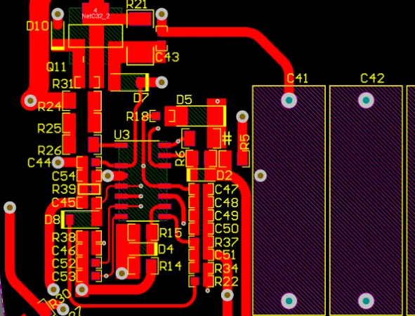
One of the biggest mixed-signal PCB DFM issues is improper grounding. Grounding is critical to managing noise and ensuring signal integrity, but many designers overlook grounding techniques DFM during the layout phase. A poorly designed ground plane can lead to ground loops, where unwanted currents flow through the ground path, introducing noise into sensitive analog circuits.
Common Mistake: Using a single ground plane for both analog and digital signals without separation. Digital circuits switch rapidly, creating high-frequency noise that can couple into analog sections through a shared ground, degrading performance. For example, a digital clock signal switching at 100 MHz can introduce noise spikes of several millivolts into an analog circuit with a shared ground.
Solution: Implement split ground planes to separate analog and digital grounds. Connect these planes at a single point, often near the power supply or ADC (Analog-to-Digital Converter), to minimize noise coupling. Ensure the split is carefully planned during the DFM stage to avoid manufacturing issues like incomplete etching or misalignment. Additionally, place ground vias strategically to provide low-impedance return paths for high-speed signals, reducing EMI.
2. Inadequate Signal Isolation in DFM
Another frequent pitfall is failing to address signal isolation DFM. Mixed-signal designs often have high-speed digital traces running near sensitive analog traces, leading to crosstalk and interference. If not considered during the DFM process, this can result in layouts that are difficult to manufacture or prone to performance issues.
Common Mistake: Routing digital and analog traces close together without proper spacing or shielding. For instance, a digital signal with a rise time of 1 ns can induce crosstalk in an adjacent analog trace if spaced less than 3 times the trace width apart, leading to signal distortion.
Solution: Maintain adequate spacing between analog and digital traces, ideally at least 3 to 5 times the trace width, depending on signal speed. Use guard traces or ground shields between critical signals to further reduce crosstalk. During the DFM review, ensure that trace spacing and layer stack-up are compatible with manufacturing capabilities, avoiding overly tight tolerances that could lead to fabrication errors. Additionally, consider placing analog components on one side of the board and digital components on the other to enhance isolation.
3. Ignoring Noise Reduction Strategies in Mixed-Signal PCBs
Noise is a constant concern in mixed-signal designs, and failing to prioritize noise reduction in mixed-signal PCBs during the DFM phase can lead to boards that perform poorly or fail entirely. Noise can come from various sources, including power supply fluctuations, digital switching, and external EMI.
Common Mistake: Neglecting proper decoupling and filtering in the layout. Without adequate decoupling capacitors near IC power pins, voltage fluctuations can introduce noise into the system. For example, a digital IC switching at 50 MHz may cause a 100 mV ripple on the power line if decoupling is insufficient, affecting nearby analog circuits.
Solution: Place decoupling capacitors as close as possible to the power pins of ICs, ideally within 0.1 inches, to minimize inductance. Use a combination of capacitor values (e.g., 0.1 μF and 10 μF) to filter a wide range of frequencies. During DFM, ensure that component placement and pad sizes are optimized for manufacturing, avoiding issues like tombstoning during soldering. Additionally, consider using ferrite beads in series with power lines to analog sections for further noise suppression. Plan the layer stack-up to include dedicated power and ground planes to reduce impedance and improve noise immunity.
4. Overlooking Component Placement for Manufacturability
Component placement is another area where mixed-signal PCB DFM issues often arise. Poor placement can lead to signal integrity problems, increased noise, and manufacturing difficulties. DFM isn’t just about functionality—it’s about ensuring the design can be built reliably.
Common Mistake: Placing analog and digital components randomly without considering signal flow or thermal management. For example, placing a high-power digital IC near a temperature-sensitive analog sensor can cause drift in sensor readings due to localized heating.
Solution: Group analog components together in a dedicated section of the board, away from noisy digital circuits. Place high-speed digital components closer to connectors to minimize trace lengths and reduce EMI. During the DFM process, check that component spacing meets manufacturing guidelines to prevent soldering issues like bridging. Also, consider thermal dissipation by spacing out heat-generating components and adding thermal vias if needed. For instance, ensure a clearance of at least 0.3 inches between high-power components to allow for proper heat dissipation.
5. Failing to Account for Layer Stack-Up in DFM
The layer stack-up in a mixed-signal PCB plays a vital role in signal integrity and noise management. Ignoring stack-up considerations during DFM can lead to designs that are prone to interference or difficult to fabricate.
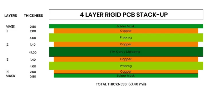
Common Mistake: Using an unbalanced or poorly planned stack-up that doesn’t prioritize ground and power planes. Without adjacent ground planes, high-speed signals can suffer from impedance mismatches, leading to reflections and signal degradation. For example, a 4-layer board without a dedicated ground plane can increase loop inductance, resulting in a noise margin reduction of up to 20%.
Solution: Design the stack-up with adjacent ground and power planes to provide low-impedance paths for return currents. For a 4-layer board, a common configuration is Signal-Ground-Power-Signal, ensuring that high-speed traces are referenced to a ground plane. During DFM, verify that the stack-up aligns with manufacturing capabilities, such as dielectric thickness and copper weight, to avoid issues like warping or delamination. If possible, use a 6-layer or higher stack-up for complex designs to allow for additional shielding layers.
Best Practices for Mixed-Signal PCB DFM
Beyond avoiding specific pitfalls, adopting best practices can elevate the quality of your mixed-signal PCB designs. Here are some actionable tips to integrate into your workflow:
- Prioritize Early DFM Reviews: Conduct DFM checks during the initial design phase to catch issues like trace spacing or component clearance before they become costly mistakes in production.
- Simulate Signal Integrity: Use simulation tools to analyze signal integrity and noise before finalizing the layout. This can help identify potential crosstalk or impedance issues early on.
- Collaborate with Manufacturers: Work closely with your PCB fabrication team to understand their capabilities and constraints. For example, confirm minimum trace widths (often 6 mils for standard processes) and via sizes to ensure manufacturability.
- Document Design Intent: Clearly document grounding schemes, isolation zones, and critical placement requirements in your design files to avoid misinterpretation during manufacturing.
Why DFM Matters for Mixed-Signal PCB Success
In mixed-signal PCB design, DFM isn’t just a box to check—it’s a fundamental part of creating reliable, high-performance boards. By addressing mixed-signal PCB DFM issues like poor grounding, inadequate isolation, and noise, you can prevent costly redesigns and ensure your product meets performance expectations. Applying proper grounding techniques DFM, focusing on signal isolation DFM, and prioritizing noise reduction in mixed-signal PCBs will set your design apart in terms of quality and reliability.
Every step, from planning split ground planes to optimizing layer stack-ups, contributes to a smoother manufacturing process and a better end product. As you refine your skills in mixed-signal design, remember that attention to DFM details can make the difference between a functional board and a failed prototype.
Conclusion
Designing mixed-signal PCBs comes with unique challenges, but by avoiding common DFM pitfalls, you can achieve outstanding results. Focus on effective grounding, proper signal isolation, and robust noise reduction strategies to ensure your boards perform as intended. With careful planning and adherence to DFM principles, you’ll minimize manufacturing issues and deliver designs that meet both technical and production requirements.
Start implementing these tips in your next project to see the difference. By mastering mixed-signal PCB DFM issues, leveraging grounding techniques DFM, optimizing signal isolation DFM, and enhancing noise reduction in mixed-signal PCBs, you’re on your way to creating high-quality, reliable designs that stand the test of time.


