 ALLPCB


When it comes to high-speed PCB design, one of the most critical factors to get right is the line width of your traces, often measured in mils (thousandths of an inch). Optimizing trace width for high-speed signals ensures signal integrity, minimizes transmission line effects, and achieves proper impedance matching. In this comprehensive guide, we’ll dive deep into advanced techniques to fine-tune line width for high-speed PCBs, helping you create designs that perform reliably even at gigahertz frequencies.
Whether you’re tackling a complex multi-layer board or refining a high-frequency application, understanding how to calculate and adjust trace widths can make or break your project. Let’s explore the strategies, tools, and considerations that go beyond the basics to elevate your PCB designs.
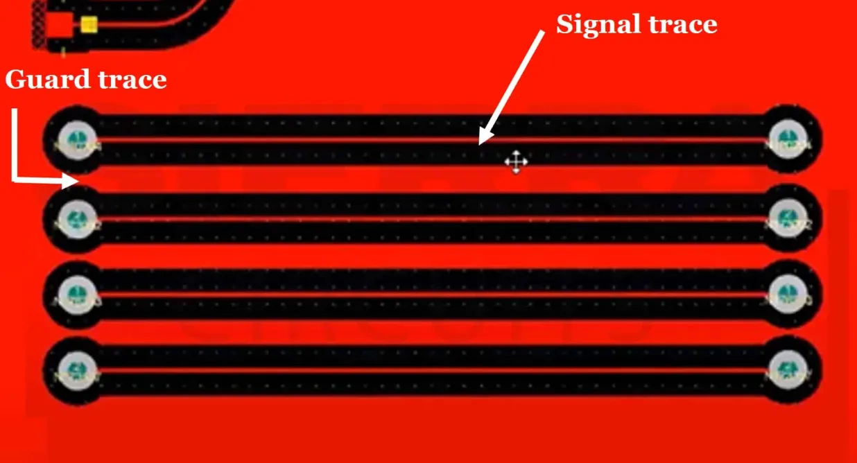
Why Line Width Matters in High-Speed PCB Design
In high-speed PCB design, the width of a trace isn’t just about fitting it on the board—it directly impacts how signals behave. Traces act as transmission lines at high frequencies, typically above 100 MHz, where signal integrity becomes a major concern. A poorly optimized trace width can lead to issues like signal reflection, crosstalk, and electromagnetic interference (EMI), all of which degrade performance.
Line width, measured in mils, influences the characteristic impedance of a trace. For instance, a typical 50-ohm impedance, common in high-speed digital circuits, requires precise control of trace width and spacing relative to the dielectric material and ground plane. If the width is off by even a few mils, the impedance mismatch can cause signal distortions. Moreover, trace width affects current-carrying capacity and heat dissipation, which are crucial for maintaining reliability in high-speed applications.
In the sections below, we’ll break down the advanced methods to optimize trace width, ensuring your design meets the stringent demands of modern electronics.
Understanding Transmission Line Effects and Signal Integrity
Before diving into optimization techniques, it’s essential to grasp how transmission line effects impact high-speed signals. At high frequencies, a PCB trace behaves like a transmission line rather than a simple conductor. This means signals propagate as waves, and any mismatch in impedance can cause reflections, leading to data errors or signal loss.
Signal integrity refers to the quality of the signal as it travels through the trace. Key factors affecting signal integrity include:
- Reflections: Caused by impedance mismatches, often due to incorrect trace width or abrupt changes in the trace path.
- Crosstalk: Interference between adjacent traces, exacerbated by narrow spacing or improper width design.
- Attenuation: Signal loss due to resistance and dielectric losses, influenced by trace width and material properties.
To mitigate these issues, optimizing trace width in mils is a foundational step. A wider trace generally reduces resistance and attenuation but can increase capacitance, altering impedance. Conversely, a narrower trace may minimize capacitance but risks higher resistance and potential overheating. Striking the right balance is key for high-speed PCB design.
Calculating Trace Width for Impedance Matching
One of the primary goals in high-speed PCB design is achieving impedance matching. Most high-speed digital signals, such as USB, HDMI, or DDR memory, require a specific characteristic impedance, often 50 ohms for single-ended signals or 100 ohms for differential pairs.
To calculate the optimal trace width for a desired impedance, you need to consider several parameters:
- Dielectric Constant (Er): The property of the PCB substrate material, typically around 4.2 for standard FR-4 material.
- Trace Height (H): The distance between the trace and the reference ground plane, determined by the PCB stack-up.
- Trace Thickness (T): Usually 1 oz copper (1.4 mils) or 2 oz copper (2.8 mils) for most designs.
- Target Impedance (Z0): The desired impedance value, such as 50 ohms.
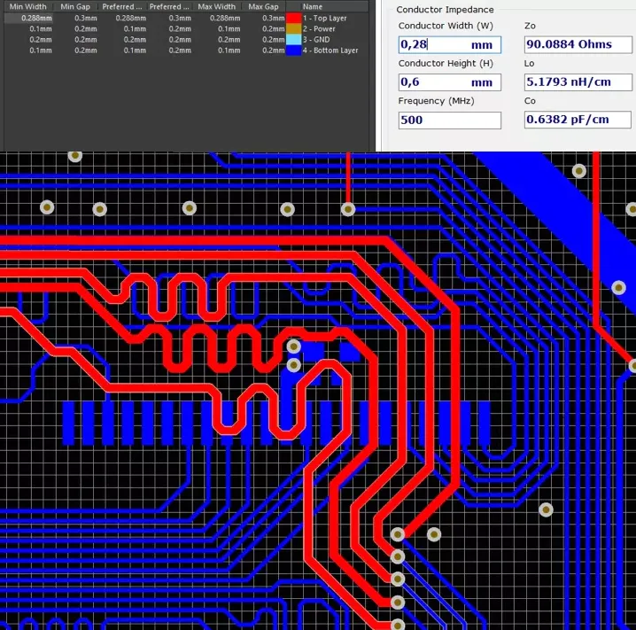
A common formula for microstrip traces (traces on the outer layer with a ground plane below) is derived from empirical models. For a 50-ohm impedance on FR-4 with a dielectric height of 10 mils and 1 oz copper, the trace width often comes out to approximately 18-20 mils. However, for precise calculations, using a field solver or impedance calculator tool is highly recommended, as manual calculations can be error-prone.
For stripline configurations (traces sandwiched between two ground planes), the width may differ due to the dual reference planes affecting capacitance. Typically, stripline traces are narrower than microstrip traces for the same impedance due to higher capacitance.
Advanced Techniques for Optimizing Trace Width
Now that we’ve covered the fundamentals, let’s explore advanced strategies to fine-tune line width in mils for high-speed PCBs. These techniques go beyond basic calculations and address real-world challenges in maintaining signal integrity and performance.
1. Adjusting Width for Frequency-Dependent Effects
At very high frequencies (above 1 GHz), skin effect and dielectric losses become significant. The skin effect causes current to concentrate near the surface of the trace, increasing effective resistance. To counteract this, slightly wider traces can help reduce losses, though this must be balanced with impedance requirements. For example, a trace width of 15 mils might be increased to 18 mils for a 5 GHz signal on FR-4 to account for these losses, assuming impedance is recalculated.
2. Differential Pair Width Optimization
For differential signaling, used in protocols like USB 3.0 or PCIe, trace width and spacing are critical. Differential pairs require matched lengths and consistent impedance, often 100 ohms. A common approach is to use a width of around 8-10 mils per trace with a spacing of 8-12 mils for a 100-ohm differential impedance on a standard 4-layer board. Adjusting width slightly can fine-tune the impedance if manufacturing tolerances introduce variations.
3. Tapering Traces for Impedance Transitions
In some high-speed designs, you may need to transition between different impedance values, such as connecting a 50-ohm trace to a 75-ohm component. Abrupt changes cause reflections, so tapering the trace width gradually over a short distance can minimize discontinuities. For instance, widening a trace from 10 mils to 15 mils over a length of 100 mils can smooth the impedance transition.
4. Considering Manufacturing Tolerances
PCB fabrication processes have tolerances that affect final trace width, typically ±10% for standard manufacturing. If you design a trace at 10 mils, the actual width might vary between 9 and 11 mils, impacting impedance. To mitigate this, work closely with your manufacturer to understand their capabilities and design with a safety margin. For critical high-speed signals, consider specifying tighter tolerances or using controlled impedance processes.
Tools for Precision in Trace Width Optimization
Manual calculations for trace width can be time-consuming and prone to errors, especially in complex designs. Leveraging specialized software tools can streamline the process and improve accuracy. Here are some approaches to consider:
- 2D Field Solvers: These tools simulate the electromagnetic fields around a trace to calculate impedance based on width, height, and material properties. They are ideal for precise high-speed PCB design.
- PCB Design Software: Many design platforms include built-in impedance calculators that suggest trace widths based on your stack-up and target impedance.
- Simulation Tools: For ultra-high-speed designs, full-wave 3D simulation software can model transmission line effects, crosstalk, and other signal integrity issues tied to trace width.
Using these tools, you can iterate on trace width values in mils until you achieve the desired performance, saving time and reducing costly redesigns.
Material and Stack-Up Considerations
Trace width optimization doesn’t happen in isolation—it’s closely tied to the PCB material and stack-up. High-speed designs often benefit from low-loss dielectric materials like Rogers or Isola, which have a lower dielectric constant (Er) and loss tangent compared to standard FR-4. For example, using a material with Er = 3.5 instead of 4.2 might allow a slightly wider trace for the same 50-ohm impedance, improving current capacity.
The stack-up design also plays a role. A thinner dielectric layer between the trace and ground plane increases capacitance, requiring a narrower trace to maintain impedance. For a 4-layer board with a 5-mil dielectric height, a 50-ohm trace might need to be as narrow as 8 mils, whereas a 10-mil height could allow for 18 mils. Always design trace width in conjunction with your stack-up plan for consistent results.
Practical Tips for High-Speed PCB Trace Width Design
To wrap up, here are some actionable tips to apply these advanced techniques in your next high-speed PCB project:
- Start with a target impedance and use a calculator or solver to determine the initial trace width in mils.
- Simulate your design to check for signal integrity issues like reflections or crosstalk, adjusting width as needed.
- Keep trace widths consistent along the signal path to avoid impedance discontinuities.
- Account for manufacturing tolerances by designing with a buffer and confirming capabilities with your fabricator.
- Prioritize controlled impedance for critical high-speed signals, specifying this requirement during fabrication.
Conclusion: Mastering Trace Width for High-Speed Success
Optimizing line width in mils for high-speed PCBs is a critical skill that separates good designs from great ones. By understanding transmission line effects, calculating trace width for impedance matching, and applying advanced techniques like differential pair optimization and tapering, you can ensure signal integrity and reliability in even the most demanding applications.
High-speed PCB design is a balance of science and art, requiring attention to detail and the right tools. With the strategies outlined in this guide, you’re equipped to tackle trace width challenges head-on, creating boards that perform at peak efficiency. From gigabit data rates to RF applications, mastering trace width optimization opens the door to cutting-edge innovation in electronics design.


