 ALLPCB


In the world of PCB assembly, achieving precision in solder paste application is critical, especially for fine-pitch components like 0201 packages and complex BGA layouts. Laser cut stencils have become the go-to solution for ensuring accurate solder paste deposition, offering unmatched control over volume and placement. If you're looking to master laser cut stencil fine pitch components or optimize solder paste volume control, this guide will walk you through the essentials of stencil design and application for modern PCB manufacturing.
In this comprehensive blog, we'll dive deep into the intricacies of stencil aperture design for 0201 components, explore BGA stencil requirements, and provide actionable insights to help you achieve flawless results in your assembly process. Whether you're an engineer or a manufacturer, you'll find practical tips and detailed explanations to elevate your production quality.
Why Laser Cut Stencils Are Essential for Fine-Pitch PCBs
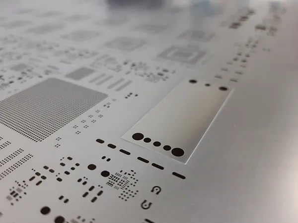
Fine-pitch PCBs, which often include components with lead spacing as small as 0.4mm or less, demand extreme precision during solder paste application. Even a slight deviation in paste volume or alignment can lead to defects like bridging, tombstoning, or insufficient solder joints. This is where laser cut stencils shine. Unlike traditional chemical-etched stencils, laser cutting offers superior accuracy, creating clean, precise apertures that match the exact requirements of modern components.
Laser cut stencils are manufactured by using a high-powered laser to cut through a thin stainless steel sheet, typically between 0.1mm and 0.15mm thick. This process ensures smooth edges and consistent aperture sizes, which are vital for controlling solder paste deposition on pads as small as those found on 0201 components (measuring just 0.6mm x 0.3mm). With laser technology, manufacturers can achieve tolerances as tight as ±0.005mm, making it an ideal choice for high-density PCB designs.
Key Benefits of Laser Cut Stencils for Solder Paste Application
Before diving into the technical details of stencil design, let's explore why laser cut stencils are the preferred choice for fine-pitch PCB assembly:
- Precision and Consistency: Laser cutting ensures that each aperture is uniform, reducing variability in solder paste volume across the board.
- Smooth Aperture Walls: The laser process creates clean, burr-free edges, allowing for better paste release and reducing the risk of clogging.
- Customizability: Laser technology can easily accommodate complex designs, including stepped stencils for mixed-component boards.
- Durability: Made from high-quality stainless steel, these stencils withstand repeated use without deforming or losing accuracy.
These advantages directly translate to improved yield rates and fewer defects in production, especially when dealing with challenging components like BGAs and ultra-small passives.
Understanding Solder Paste Volume Control with Laser Cut Stencils
One of the most critical aspects of stencil design is solder paste volume control. Too much paste can cause bridging between pads, while too little can result in weak or open solder joints. For fine-pitch components, controlling this volume becomes even more challenging due to the tiny pad sizes and tight spacing.
The volume of solder paste deposited on a pad is determined by the stencil's aperture size and thickness. A general rule of thumb is to aim for a paste volume that covers 80-90% of the pad area after reflow, accounting for the natural spread and collapse of the paste during heating. For instance, a typical 0201 component pad might require an aperture width of 0.25mm and a stencil thickness of 0.1mm to achieve the optimal paste volume of approximately 0.006 cubic millimeters.
To fine-tune solder paste volume, engineers often adjust the aperture design. Reducing the aperture size by 10-20% compared to the pad size (known as aperture reduction) can prevent excess paste, while maintaining a 1:1 ratio might be necessary for larger pads or high-power components requiring more solder.
Stencil Aperture Design for 0201 Components
When it comes to stencil aperture design for 0201 components, precision is non-negotiable. These tiny components, measuring just 0.6mm x 0.3mm, have pads that are incredibly small, often around 0.3mm x 0.3mm or smaller after accounting for tolerances. Designing apertures for such components requires careful consideration of several factors:
- Aperture Shape: Rounded or trapezoidal apertures are often preferred over square ones for 0201 components. Rounded corners improve paste release by reducing surface tension at the edges, ensuring a cleaner deposit.
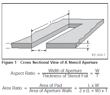
- Area Ratio: The area ratio, defined as the aperture opening area divided by the wall area of the aperture, should ideally be above 0.66 for consistent paste transfer. For 0201 pads, this often means using a thinner stencil (e.g., 0.08mm) to maintain a favorable ratio.
- Spacing: With pad spacing as tight as 0.2mm, apertures must be precisely aligned to avoid bridging. Laser cutting allows for exact placement, minimizing misalignment risks.
In practice, a common approach for 0201 components is to use a stencil thickness of 0.08mm to 0.1mm with a slight aperture reduction (e.g., 10%) to control paste volume. This setup helps achieve reliable solder joints without excess paste spilling over to adjacent pads.
BGA Stencil Requirements for Optimal Performance
Ball Grid Array (BGA) components present unique challenges due to their high pin count and hidden connections beneath the package. Meeting BGA stencil requirements is essential to ensure proper solder joint formation and avoid issues like voids or insufficient solder.
For BGA components, stencil design focuses on achieving uniform paste deposition across hundreds or thousands of tiny pads, often with pitches as fine as 0.4mm. Here are the key considerations for BGA stencil design:
- Aperture Size and Shape: BGA apertures are typically circular to match the spherical shape of solder balls. The aperture diameter is often set to 80-90% of the pad diameter to prevent excess paste, which could lead to bridging during reflow. For a 0.5mm pitch BGA, an aperture diameter of 0.25mm to 0.3mm is common.
- Stencil Thickness: A thickness of 0.1mm to 0.15mm is standard for most BGAs, balancing paste volume with ease of release. Thicker stencils may be used for larger BGAs requiring more solder.
- Alignment Precision: Misalignment by even 0.05mm can cause solder paste to miss BGA pads entirely. Laser cut stencils, with their high precision, ensure accurate alignment, often aided by fiducial marks on the PCB and stencil.
- Void Prevention: To reduce voids in BGA solder joints, some designs incorporate micro-apertures or split patterns within a single pad area to allow better outgassing during reflow.
By adhering to these guidelines, manufacturers can achieve consistent BGA soldering results, even on densely populated boards with fine-pitch layouts.
Best Practices for Using Laser Cut Stencils in Production
Even with a perfectly designed stencil, success in solder paste application depends on proper handling and process control during production. Here are some best practices to ensure optimal results with laser cut stencils for fine-pitch PCBs:
- Stencil Cleaning: Regularly clean the stencil using an ultrasonic cleaner or automated stencil cleaning system to remove residual paste. Buildup in apertures, especially for fine-pitch designs, can lead to inconsistent deposits.
- Squeegee Pressure and Angle: Use a squeegee angle of 45-60 degrees and apply moderate pressure (around 3-5 kg for a 300mm squeegee) to ensure even paste distribution without damaging the stencil.
- Paste Selection: Choose a solder paste with a particle size suitable for fine-pitch apertures. Type 4 or Type 5 paste, with particle sizes of 20-38 microns or 15-25 microns respectively, works best for 0201 and BGA components.
- Inspection: Use a solder paste inspection (SPI) system to verify paste volume and alignment after printing. Modern SPI tools can detect deviations as small as 10% in volume, helping catch issues before reflow.
Implementing these practices can significantly reduce defects and improve the reliability of your PCB assemblies, especially for high-density designs.
Common Challenges and How to Overcome Them
While laser cut stencils offer many advantages, certain challenges can arise during their use with fine-pitch components. Here's how to address some common issues:
- Paste Bridging: If bridging occurs between fine-pitch pads, consider reducing the aperture size by 10-15% or lowering the stencil thickness to limit paste volume. Ensure proper squeegee pressure to avoid over-deposition.
- Poor Paste Release: For 0201 or smaller apertures, poor release can result from a low area ratio. Switching to a thinner stencil or using a nano-coated stencil can improve paste transfer efficiency.
- Misalignment: Use high-precision alignment systems and fiducial marks to ensure the stencil aligns perfectly with the PCB. Laser cut stencils often include alignment features for this purpose.
By anticipating these challenges and adjusting your stencil design or process parameters, you can maintain high-quality solder paste application even on the most complex boards.
Conclusion: Elevate Your PCB Assembly with Precision Stencils
Mastering laser cut stencil fine pitch components is a game-changer for modern PCB assembly. By focusing on solder paste volume control, optimizing stencil aperture design for 0201 components, and meeting BGA stencil requirements, you can achieve consistent, high-quality results in your production line. Laser cut stencils provide the precision and flexibility needed to tackle the challenges of fine-pitch designs, ensuring reliable solder joints and minimal defects.
At ALLPCB, we're committed to supporting engineers and manufacturers with cutting-edge solutions for PCB assembly. By leveraging the power of laser cut stencils and following the best practices outlined in this guide, you can take your production process to the next level. Precision in solder paste application is not just a goal—it's a necessity for success in today's competitive electronics industry.


