 ALLPCB


Are you looking to streamline your PCB design for automated assembly while ensuring manufacturability and cost-efficiency? The key lies in mastering Design for Manufacturing (DFM) with a focus on Design for Assembly (DFA). In this guide, we’ll dive into practical strategies like component placement guidelines, via design, solder mask design, and panelization to help you create PCBs that are easier and cheaper to produce without sacrificing quality. Let’s explore how to optimize your designs step by step for electric engineers seeking actionable insights.
Introduction: Why DFM and DFA Matter in PCB Design
For electric engineers, designing a printed circuit board (PCB) isn’t just about functionality—it’s about ensuring that the board can be manufactured and assembled efficiently. Design for Manufacturing (DFM) focuses on creating a PCB layout that minimizes production issues, while Design for Assembly (DFA) ensures that the assembly process, especially automated assembly, is smooth and error-free. Together, these principles reduce costs, speed up production, and improve product reliability.
In today’s fast-paced electronics industry, automated assembly is the norm for high-volume production. However, poorly optimized designs can lead to assembly errors, increased rework, and higher costs. By following DFM and DFA guidelines, you can avoid common pitfalls and ensure your PCB is ready for the pick-and-place machines and soldering processes. Let’s break down the critical aspects of optimizing your PCB design for automated assembly, focusing on component placement guidelines, via design, solder mask design, and panelization.

What is Design for Assembly (DFA) in PCB Design?
Design for Assembly (DFA) is a set of guidelines aimed at simplifying the assembly process of a PCB. For automated assembly, DFA is crucial because it ensures that components can be placed and soldered by machines with minimal errors. DFA focuses on reducing the number of assembly steps, minimizing manual intervention, and optimizing the layout for machine precision.
Key DFA principles include using standard component sizes, ensuring proper spacing for pick-and-place machines, and aligning components in a uniform orientation. For example, aligning all polarized components (like capacitors or diodes) in the same direction can reduce errors during automated placement. According to industry standards, maintaining a minimum spacing of 0.5 mm between components can prevent issues with machine accuracy during placement.
By integrating DFA into your workflow, you can reduce assembly time by up to 30% and cut down on costly rework. This is especially important for high-volume production where even small inefficiencies can add up quickly.
Component Placement Guidelines for Automated Assembly
One of the most critical aspects of DFA is component placement. Poor placement can lead to assembly errors, soldering defects, and even functional failures. Here are some actionable component placement guidelines to follow:
- Uniform Orientation: Place components like resistors, capacitors, and ICs in the same orientation to simplify programming for pick-and-place machines. For instance, ensure all IC pins face the same direction.
- Spacing and Clearance: Maintain a minimum clearance of 0.5 mm between components to avoid interference during automated placement. For high-density designs, consider using a 0.8 mm clearance for added safety.
- Edge Clearance: Keep components at least 3 mm away from the PCB edges to prevent damage during depanelization and to allow space for handling by automated equipment.
- Height Considerations: Group components of similar heights together to avoid shadowing during wave soldering. For example, place taller components like electrolytic capacitors away from shorter ones to ensure even heat distribution.
- Fiducial Marks: Include at least two fiducial marks (small copper dots) on opposite corners of the PCB. These help automated assembly machines align the board accurately, reducing placement errors by up to 20%.
Following these guidelines ensures that your PCB is compatible with automated assembly systems, reducing the risk of misplacement and improving overall yield.
Via Design: Balancing Functionality and Manufacturability
Vias are essential for connecting different layers of a PCB, but improper via design can cause manufacturing issues and affect automated assembly. Here’s how to optimize via design for DFM:
- Minimize Via Types: Stick to standard via sizes (e.g., 0.3 mm drill diameter with a 0.6 mm pad) to simplify drilling and plating processes. Using non-standard sizes can increase manufacturing costs by 15-20%.
- Avoid Vias in Pads: Placing vias in component pads (via-in-pad) can lead to solder wicking during reflow, causing poor connections. If unavoidable, use filled and capped vias, though this increases costs.
- Spacing from Components: Keep vias at least 0.3 mm away from component pads to prevent interference during soldering. This spacing also reduces the risk of thermal stress on nearby components.
- Tenting or Covering Vias: Cover vias with solder mask (tenting) to prevent solder paste from flowing into them during assembly. Uncovered vias near SMT pads can cause shorts or uneven soldering.
Proper via design not only improves manufacturability but also enhances the reliability of your PCB by reducing defects during automated assembly. For high-speed designs, ensure vias don’t interfere with signal integrity—keep them away from critical traces carrying signals above 100 MHz.
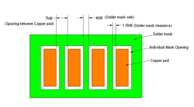
Solder Mask Design: Ensuring Precision and Protection
Solder mask design plays a vital role in protecting your PCB during automated assembly and ensuring precise soldering. A poorly designed solder mask can lead to solder bridges, insufficient coverage, or misalignment. Here’s how to optimize solder mask design:
- Clearance Around Pads: Maintain a solder mask clearance of 0.1 mm around SMT pads to prevent mask overlap, which can interfere with solder paste application. For fine-pitch components (below 0.5 mm pitch), consider a 0.05 mm clearance for precision.
- Avoid Mask on Vias Near Pads: As mentioned earlier, tent vias near pads to prevent solder flow issues. However, for test points or vias not near pads, leaving them uncovered can reduce manufacturing costs.
- Alignment Tolerance: Account for a solder mask alignment tolerance of ±0.05 mm during design. Misalignment can expose copper and lead to shorts, as highlighted in posts found on social platforms like X where engineers shared real-world examples of solder mask issues causing hidden solder bridges.
- Use Standard Colors: Stick to standard solder mask colors like green or blue unless specified by the client. Non-standard colors can increase costs and lead times by 10-15% due to special material requirements.
A well-designed solder mask ensures that your PCB withstands the rigors of automated assembly while maintaining electrical isolation and preventing soldering defects. Always double-check your design files using DFM analysis tools to catch potential solder mask issues before production.
Panelization: Maximizing Efficiency in Manufacturing
Panelization is the process of grouping multiple PCBs onto a single panel for manufacturing and assembly. Proper panelization is a cornerstone of DFM, as it reduces material waste, speeds up production, and simplifies handling during automated assembly. Here’s how to optimize panelization:
- Standard Panel Sizes: Design your panel to fit standard sizes like 18 x 24 inches to maximize compatibility with most manufacturers’ equipment. Non-standard sizes can increase costs by 20% or more.
- Breakaway Tabs: Use breakaway tabs (mouse bites) or V-scoring to separate individual PCBs from the panel after assembly. Ensure tabs are at least 3 mm wide to prevent damage during depanelization.
- Tooling Holes: Include at least three non-plated tooling holes (3 mm diameter) on the panel for alignment during automated assembly. Place them near the corners for stability.
- Spacing Between Boards: Maintain a minimum spacing of 2.5 mm between individual PCBs on the panel to allow for clean separation and to accommodate manufacturing tolerances.
- Fiducials on Panel: Add global fiducial marks on the panel itself (in addition to individual PCB fiducials) to assist automated machines in aligning the entire panel accurately.
Effective panelization can reduce manufacturing costs by up to 25% by optimizing material usage and minimizing setup time for automated assembly lines. Always consult with your manufacturer to confirm panelization requirements before finalizing your design.
Additional DFM Tips for Automated Assembly
Beyond the core areas of DFA, component placement, via design, solder mask, and panelization, here are a few additional DFM tips to ensure your PCB design is fully optimized for automated assembly:
- Standardize Components: Use widely available components with standard footprints to avoid supply chain delays and compatibility issues with assembly equipment.
- Minimize Manual Assembly: Avoid components that require manual placement or soldering, as they slow down automated processes and increase labor costs by up to 40%.
- Thermal Relief Pads: Use thermal relief pads for through-hole components to ensure even heat distribution during soldering, reducing the risk of cold solder joints.
- DFM Analysis Tools: Leverage software tools like Cadence Allegro or Altium Designer to run DFM checks before sending your design to production. These tools can flag issues like insufficient clearances or unmanufacturable features.
Implementing these tips can further enhance the manufacturability of your PCB, saving time and money while ensuring high-quality results.
Common Pitfalls to Avoid in PCB Design for Automated Assembly
Even with the best intentions, certain design oversights can derail your automated assembly process. Here are some common pitfalls to watch out for:
- Ignoring Manufacturer Guidelines: Every manufacturer has specific DFM and DFA requirements. Failing to follow them can lead to production delays or rejected boards.
- Overcrowded Layouts: Cramming too many components into a small area might save space but often results in assembly errors and thermal issues.
- Inadequate Testing Points: Not including enough test points can make post-assembly testing difficult, leading to undetected defects.
- Poor Documentation: Incomplete or unclear assembly instructions can cause confusion, especially if manual steps are involved. Provide detailed BOMs and assembly drawings.
By being mindful of these pitfalls, you can avoid costly mistakes and ensure a smoother transition from design to production.
Conclusion: Streamlining Your PCB Design with DFM and DFA
Optimizing your PCB design for automated assembly is a critical step in achieving efficient, cost-effective production. By focusing on Design for Assembly (DFA) principles, adhering to component placement guidelines, refining via design, perfecting solder mask design, and implementing effective panelization, you can significantly improve the manufacturability of your boards. These strategies not only reduce errors during automated assembly but also save time and lower costs, which is a win for any electric engineer or design team.
Start by integrating these DFM practices into your next project. Use DFM analysis tools, consult with your manufacturer, and continually refine your approach based on feedback from production runs. The result? High-quality PCBs that are easier to assemble and built to last.


