 ALLPCB


Introduction
In modern PCB designs, especially those handling high-speed digital signals or sensitive analog circuits, electromagnetic interference (EMI) and crosstalk pose significant challenges to signal integrity. These issues can degrade performance, cause data errors, and lead to compliance failures in electromagnetic compatibility testing. Via fences emerge as a proven passive shielding technique to address these problems by creating barriers that contain electromagnetic fields. Engineers often implement via fences around critical traces or components to isolate noise sources and victims effectively. This article explores the design principles, implementation strategies, and effectiveness of via fences in minimizing EMI and crosstalk. By understanding via fence spacing, via fence grounding, and related factors, designers can enhance PCB reliability in demanding applications.
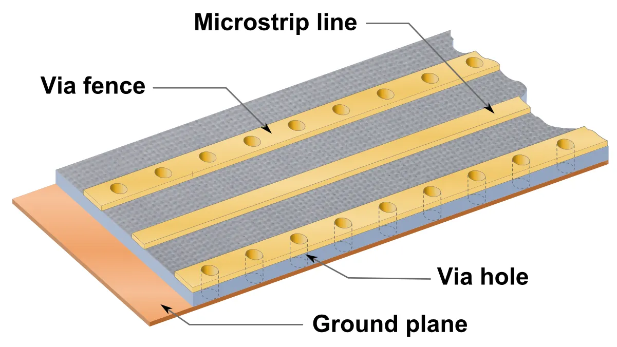
What Is a Via Fence and Why It Matters
A via fence consists of a closely spaced array of grounded vias arranged along a trace or around a circuit area on a multilayer PCB. These vias connect to ground planes on multiple layers, forming a continuous electromagnetic shield that blocks field propagation. Unlike solid metal shields, via fences leverage the PCB's layered structure for cost-effective isolation without adding external components. In high-frequency environments, such as RF modules or SerDes interfaces, uncontrolled EMI can radiate from clock lines or power planes, coupling into nearby signals. Crosstalk, arising from mutual inductance or capacitance between adjacent traces, further compromises integrity in dense layouts.
The relevance of via fences grows with increasing data rates and miniaturization in PCBs. Sensitive circuits, including ADCs, amplifiers, or high-speed serializers, demand low noise floors to maintain accuracy and bit error rates. Without proper shielding, EMI reduction via fencing becomes essential to prevent radiated emissions that violate regulatory limits. Similarly, crosstalk prevention via fence configurations help maintain signal-to-noise ratios in mixed-signal boards. Industry standards like IPC-2221 emphasize controlled spacing and grounding in high-speed designs to ensure performance. Ultimately, via fences offer a balance of simplicity and effectiveness for electric engineers tackling signal integrity issues.
Technical Principles Behind Via Fence Effectiveness
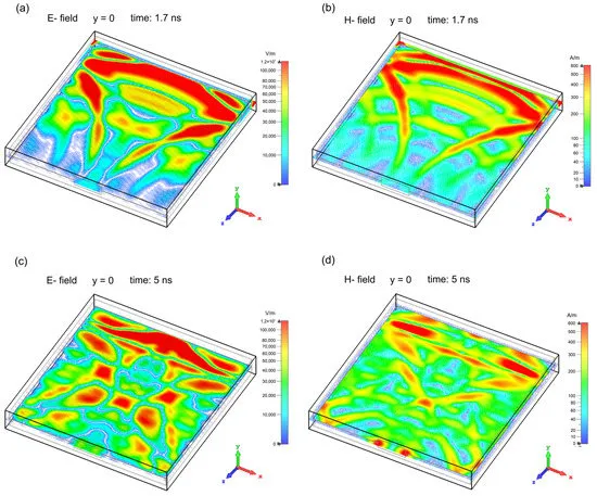
Via fences operate on electromagnetic principles where arrays of grounded vias approximate a continuous conducting wall at frequencies below a cutoff determined by spacing. At high frequencies, the fence acts as a periodic structure, creating stopbands that attenuate propagating waves. Electromagnetic fields from a noisy trace induce currents on the fence vias, which reradiate oppositely to cancel the original field beyond the barrier. This shielding relies on the skin effect, confining currents to via surfaces, and the low impedance path provided by stitched ground planes. For optimal via fence effectiveness, the design must consider wavelength-dependent behavior to avoid resonances that could amplify emissions.
EMI Reduction via Fencing
EMI reduction via fencing primarily targets radiated coupling between distant board sections. A properly spaced via fence reflects or absorbs plane waves, preventing leakage through apertures in ground planes. The fence's inductance and capacitance form a low-pass filter for common-mode currents, shunting them to ground before radiation. In multilayer boards, stitching vias tie planes together, eliminating slots that act as radiating antennas. Studies show that dense via placement enhances attenuation, with effectiveness peaking when spacing aligns with signal harmonics. Engineers must model fields using Maxwell's equations to predict shielding in 3D structures.
Crosstalk Prevention via Fence
Crosstalk prevention via fence works by confining near-fields around aggressor traces, reducing inductive and capacitive coupling to victims. The grounded vias short-circuit electric fields across layers and provide return paths that minimize loop areas for magnetic fields. Forward crosstalk drops significantly as the fence disrupts evanescent waves that would otherwise propagate. Backward crosstalk sees similar benefits from image currents induced on the fence. In parallel bus routing, fences between traces limit inter-channel interference, preserving eye diagrams. The mechanism proves robust across microstrip and stripline configurations.
Related Reading: Optimizing Via-to-Via Spacing for Enhanced Signal Integrity in High-Speed PCBs
Key Design Parameters: Via Fence Spacing and Grounding
Via Fence Spacing
Via fence spacing determines the cutoff frequency above which shielding degrades, as larger gaps allow wave propagation like a slotted waveguide. Engineers calculate spacing based on the highest harmonic of interest, ensuring it remains small relative to the wavelength for opaque shielding. Too wide spacing permits slot modes, increasing EMI escape, while excessive density raises parasitic capacitance on signal lines. Practical rules derive from array theory, balancing attenuation with fabrication limits like drill sizes. In high-speed PCBs, iterative simulation refines spacing for target isolation levels. Adhering to such parameters maximizes via fence effectiveness across operating bands.
Via Fence Grounding
Via fence grounding connects all vias to solid ground planes, minimizing return path impedance for noise currents. Multiple plane stitching ensures low-inductance paths, preventing ground bounce that could couple back to signals. Placement near edges or sensitive zones ties planes, forming Faraday-like cages. Poor grounding, such as isolated islands, defeats the purpose by creating high-impedance nodes. Best practices include thermal reliefs for manufacturability while maintaining electrical continuity. Standards like IPC-6012DS guide qualification for such structures in rigid boards.
Related Reading: The Impact of Via Design on Signal Integrity in High Frequency PCBs
Practical Solutions and Best Practices
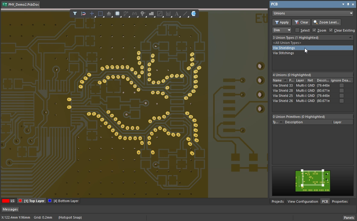
Implementing via fences starts with identifying noise sources and victims during schematic review. Route sensitive traces first, then surround them with guard traces tied to ground pours. Place vias at regular intervals along the fence length, extending beyond the trace ends to capture fringing fields. For multilayer boards, stagger vias across layers to avoid alignment holes that weaken shielding. Combine fences with orthogonal routing on adjacent layers to further suppress broadside coupling. During layout, verify spacing with frequency-domain analysis tools to confirm EMI reduction via fencing targets.
In fabrication, specify via types like through-hole or blind to match stackup needs, ensuring plating integrity per IPC guidelines. Post-layout, extract parasitics for time-domain simulations checking crosstalk prevention via fence performance. Prototype testing with near-field probes quantifies isolation before production. For dense boards, optimize via diameter to minimize inductance without excessive copper consumption. Layer sequencing with ground-signal-ground minimizes enclosure modes. These steps yield reliable designs for electric engineers.
Consider environmental factors like temperature variations affecting material properties, though via fences remain stable due to mechanical fixation. In power-sensitive applications, assess added via capacitance on driver loading. Scale fence height by including more layers for deeper shielding. Troubleshooting failures often traces to overlooked harmonics or incomplete plane stitching.
Case Study Insights: High-Speed Interface Isolation
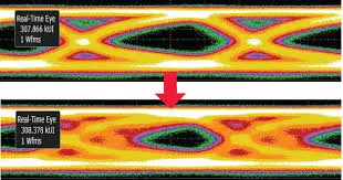
Consider a typical 10 Gbps SerDes channel on a 6-layer PCB prone to crosstalk from adjacent lanes. Without mitigation, near-end crosstalk exceeded -30 dB, violating eye mask margins. Implementing a via fence with optimized spacing around the victim lane dropped coupling to below -50 dB, restoring signal quality. Grounding to inner planes eliminated plane resonance peaks observed in scans. Simulations correlated well with measurements, validating via fence effectiveness. Adjustments for via fence grounding addressed minor loading effects. This approach scaled to full backplanes, enhancing overall EMI compliance.
Conclusion
Via fences provide electric engineers with a versatile tool for minimizing EMI and crosstalk in sensitive PCB circuits. Key elements like via fence spacing and via fence grounding directly influence shielding performance, demanding careful design tied to operating frequencies. EMI reduction via fencing and crosstalk prevention via fence integrate seamlessly into multilayer layouts, supporting high-speed and mixed-signal requirements. Following structured best practices ensures via fence effectiveness without excessive complexity. As PCB densities rise, mastering these techniques upholds signal integrity and reliability. Designers should prioritize modeling and verification for optimal results.
FAQs
Q1: What is the ideal via fence spacing for EMI reduction in high-speed PCBs?
A1: Via fence spacing should scale with the wavelength of the highest frequency component, typically kept small to form an effective barrier. Engineers base it on λ/20 rules from electromagnetic theory to block propagating waves. Proper spacing ensures the fence appears continuous, maximizing EMI reduction via fencing. Fabrication constraints and simulations refine the value for specific stackups. This approach maintains isolation across harmonics.
Q2: How does via fence grounding improve crosstalk prevention?
A2: Via fence grounding provides low-impedance paths for noise currents, shorting fields before they couple to adjacent traces. Connecting to multiple planes prevents slotline modes and ground discontinuities. Crosstalk prevention via fence relies on this to minimize both inductive and capacitive transfer. Stitching enhances return current flow, reducing loop areas. Verification through S-parameter analysis confirms improvements.
Q3: Why is via fence effectiveness frequency-dependent?
A3: Via fence effectiveness peaks below the cutoff set by spacing, acting as a stopband filter for higher frequencies. At low frequencies, it shields via field cancellation; above cutoff, gaps allow leakage. Designers target harmonics for broadband performance. Simulations predict behavior, guiding adjustments. This principle underpins reliable EMI and crosstalk control in sensitive circuits.
Q4: When should engineers use via fences in PCB design?
A4: Use via fences around high-speed traces, RF sections, or analog blocks near digital noise. They excel in multilayer boards with ground planes for stitching. Prioritize for compliance-critical applications. Combine with other techniques like guard traces for comprehensive isolation. Via fence effectiveness shines in dense layouts where traditional shielding is impractical.
References
IPC-2221B — Generic Standard on Printed Board Design. IPC, 2009
IPC-6012DS — Qualification and Performance Specification for Rigid Printed Boards. IPC, 2015
IEC 61000-5-2 — Electromagnetic compatibility (EMC) — Part 5-2: Installation and mitigation guidelines — Screening, filtering and surge suppressors. IEC, 2001


