 ALLPCB


If you're facing issues with SMT solder joints like solder bridging, insufficient solder, cold solder joints, or solder balling, you're not alone. These problems can disrupt the reliability of your PCB assembly, leading to circuit failures or costly rework. In this comprehensive guide, we'll walk you through the common solder joint issues in Surface Mount Technology (SMT) assembly, their causes, and practical solutions to fix them. Whether you're an engineer or a technician, you'll find actionable tips to improve your SMT process and ensure high-quality results.
What Are SMT Solder Joints and Why Do They Matter?
SMT solder joints are the critical connections that secure surface-mounted components to a printed circuit board (PCB). These joints ensure electrical conductivity and mechanical stability, making them the backbone of modern electronics. However, when issues like solder bridging, insufficient solder, cold solder joints, or solder balling occur, they can lead to short circuits, weak connections, or even complete failure of the device.
Understanding and troubleshooting these problems is essential for maintaining the quality of your PCB assembly. With the trend toward miniaturization and higher component density in electronics, even small defects in SMT solder joints can have significant consequences. Let's dive into the most common issues and how to address them.
Common Solder Joint Problems in SMT Assembly
Solder joint defects can arise from various factors, including improper equipment setup, incorrect materials, or environmental conditions. Below, we explore the primary issues affecting SMT solder joints and provide insights into their causes and solutions.
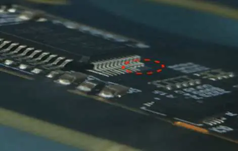
1. Solder Bridging: Unwanted Connections
Solder bridging occurs when excess solder creates an unintended connection between two or more conductors, leading to electrical shorts. This defect can cause a circuit to malfunction or fail entirely, especially in densely populated PCBs.
Causes of Solder Bridging:
- Excessive solder paste deposition during printing, often due to a high stencil aperture-to-pad ratio.
- Misalignment between the stencil and PCB pads, causing solder paste to spread beyond the intended area.
- Solder paste slump, which happens when the paste's metal-to-flux weight ratio is incorrect or when high temperature and humidity affect the paste's viscosity.
- Inadequate spacing between component pads, common in high-density designs.
Solutions for Solder Bridging:
- Optimize the solder paste printing process by ensuring proper stencil alignment and using the correct aperture size. A typical aperture-to-pad ratio of 1:1 or slightly less can help control paste volume.
- Use a solder paste with the right viscosity and store it in a controlled environment to prevent slumping. Ideal storage conditions are between 2-10°C with low humidity.
- Review PCB design to ensure adequate spacing between pads, especially for fine-pitch components (e.g., 0.5mm or less).
- Inspect and clean stencils regularly to avoid paste buildup that could lead to bridging.
2. Insufficient Solder: Weak or Missing Connections
Insufficient solder happens when there isn't enough solder material to form a proper joint between the component lead and the PCB pad. This can result in poor electrical conductivity and mechanical weakness, leading to intermittent connections or complete failure over time.
Causes of Insufficient Solder:
- Inadequate solder paste volume during printing, often due to clogged stencil apertures or incorrect stencil thickness (e.g., a stencil thinner than 0.1mm for fine-pitch components).
- Poor wetting of the solder due to contaminated pads or component leads, preventing proper adhesion.
- Incorrect reflow oven temperature profiles, where the peak temperature (e.g., below 220°C for lead-free solder) isn't high enough to fully melt the solder paste.
- Component misalignment during placement, reducing contact between the lead and solder paste.
Solutions for Insufficient Solder:
- Verify the stencil design and ensure apertures are clear. For fine-pitch components, use a stencil thickness of 0.1-0.15mm to deposit adequate paste.
- Clean PCB pads and component leads before assembly to remove oxidation or contaminants. A pre-assembly bake at 125°C for 4 hours can help remove moisture from components.
- Adjust the reflow profile to match the solder paste specifications. For lead-free solder, aim for a peak temperature of 235-245°C for 30-60 seconds.
- Use automated optical inspection (AOI) systems to detect and correct component misalignment before reflow.
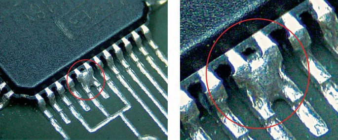
3. Cold Solder Joint: Unreliable and Brittle Connections
A cold solder joint, also known as pseudo soldering, is a defective connection where the solder hasn't properly bonded with the component lead or pad. These joints often appear dull, grainy, or lumpy and can lead to unreliable electrical connections or mechanical failure under stress.
Causes of Cold Solder Joints:
- Insufficient heat during the reflow process, preventing the formation of strong intermetallic compounds (IMCs) between the solder and metal surfaces.
- Movement or vibration of the PCB during soldering, disrupting the cooling process and leading to cracks or weak bonds.
- Use of expired or low-quality solder paste, which may not flow or wet properly.
- Poor thermal design of the PCB, where heat dissipation is uneven, causing some areas to cool too quickly.
Solutions for Cold Solder Joints:
- Ensure the reflow oven reaches the correct temperature for the solder paste used. For example, lead-free solder often requires a soak zone at 150-180°C for 60-90 seconds before peaking at 235-245°C.
- Secure the PCB during soldering to prevent any movement or vibration. Use proper fixtures or conveyors in automated assembly lines.
- Check the shelf life and storage conditions of solder paste. Discard paste older than 6 months or stored improperly.
- Optimize PCB design for thermal balance by adding thermal reliefs or adjusting copper pour areas to ensure even heating.
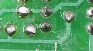
4. Solder Balling: Unwanted Solder Spheres
Solder balling refers to the formation of small, stray solder spheres on the PCB surface during the reflow process. These balls can cause shorts or interfere with component placement, posing a risk to circuit reliability.
Causes of Solder Balling:
- Excessive moisture in the solder paste or PCB, which vaporizes during reflow and scatters solder particles. This often happens when materials are stored in humid conditions (above 60% relative humidity).
- Improper solder paste printing, leading to paste outside the pad areas that forms balls during reflow.
- Too rapid a temperature ramp-up in the reflow oven (e.g., exceeding 2°C per second), causing solder paste to spatter.
- Oxidation of solder paste or PCB pads, reducing wettability and causing solder to bead up.
Solutions for Solder Balling:
- Store solder paste and PCBs in a dry, controlled environment. Pre-bake PCBs at 100-125°C for 2-4 hours to remove absorbed moisture before assembly.
- Ensure accurate solder paste printing by using well-designed stencils and inspecting for over-paste or misalignment.
- Adjust the reflow profile to include a gradual ramp-up rate of 1-2°C per second to prevent solder spattering.
- Use fresh solder paste and clean PCB pads to minimize oxidation. Nitrogen reflow atmospheres can also reduce oxidation during soldering.
General Tips for Preventing Solder Joint Issues in SMT Assembly
While addressing specific defects is crucial, implementing best practices in your SMT process can prevent many solder joint problems from occurring in the first place. Here are some universal strategies to enhance the quality of your PCB assembly:
- Invest in Quality Equipment: Use high-precision stencil printers and pick-and-place machines to ensure accurate solder paste application and component placement.
- Regular Maintenance: Clean and inspect stencils, reflow ovens, and other equipment regularly to avoid contamination or inconsistent performance.
- Monitor Environmental Conditions: Maintain a controlled assembly environment with temperatures between 20-25°C and humidity below 50% to prevent moisture-related issues.
- Use Inspection Tools: Implement automated optical inspection (AOI) and X-ray inspection systems to detect defects like solder bridging or insufficient solder early in the process.
- Train Your Team: Ensure operators and technicians are well-trained in SMT assembly techniques and troubleshooting methods to minimize human error.
How to Diagnose Solder Joint Problems Effectively
Identifying the root cause of solder joint issues is the first step to fixing them. Follow these diagnostic steps to pinpoint problems in your SMT assembly process:
- Visual Inspection: Use a magnifying glass or microscope to check for visible defects like solder bridging, cold solder joints, or solder balling. Look for dull, cracked, or uneven joints.
- Electrical Testing: Perform continuity tests to detect open circuits (from insufficient solder) or shorts (from solder bridging) using a multimeter.
- Thermal Imaging: Use thermal cameras to identify uneven heat distribution during reflow, which could lead to cold solder joints.
- X-Ray Inspection: For hidden joints or fine-pitch components, X-ray systems can reveal voids, insufficient solder, or misalignment beneath the surface.
Conclusion: Mastering SMT Solder Joint Quality
Troubleshooting solder joint problems in SMT assembly doesn't have to be overwhelming. By understanding the causes of common issues like solder bridging, insufficient solder, cold solder joints, and solder balling, you can take targeted steps to prevent and fix these defects. From optimizing your solder paste printing and reflow profiles to maintaining a controlled assembly environment, every detail matters in achieving reliable SMT solder joints.
With the practical solutions and tips provided in this guide, you're well-equipped to tackle solder joint challenges and improve the quality of your PCB assemblies. Consistent attention to detail and proactive process improvements will ensure your electronics perform reliably, meeting the demands of today's high-density, miniaturized designs.
At ALLPCB, we’re committed to supporting your PCB assembly needs with high-quality materials, advanced manufacturing processes, and expert guidance. Let’s work together to build electronics that stand the test of time.


