ALLPCB


If you're diving into manual SMT (Surface Mount Technology) assembly, creating a solder paste stencil is a crucial step for achieving precise and efficient results. A well-designed stencil ensures accurate solder paste application, which is vital for proper component placement and soldering. In this comprehensive guide, we'll walk you through the process of making a solder paste stencil DIY style, focusing on manual SMT assembly stencil techniques, PCB stencil making, stencil design for SMT, and effective solder paste application methods. Whether you're a hobbyist or a small-scale producer, this blog will provide actionable steps to help you succeed.
Why Solder Paste Stencils Matter in Manual SMT Assembly
In manual pick and place assembly, a solder paste stencil acts as a template to deposit solder paste onto the pads of a printed circuit board (PCB) with precision. Without a stencil, applying solder paste by hand can lead to uneven deposits, misplaced paste, or insufficient amounts, all of which can cause soldering defects like bridges or weak joints. A stencil ensures consistency, saves time, and improves the quality of your assembly, even when working on small batches or prototypes.
By using a manual SMT assembly stencil, you can achieve results close to automated processes while keeping costs low. Let’s explore how to create and use one effectively for your projects.
Understanding the Basics of Solder Paste Stencils
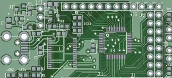
Before diving into PCB stencil making, it’s important to understand what a solder paste stencil is and how it works. A stencil is typically a thin sheet of material, often stainless steel or durable plastic like Mylar, with cutouts (apertures) that match the layout of the pads on your PCB. These apertures allow solder paste to be pushed through onto the board in the exact locations where components will be placed.
Stencils for manual assembly are often frameless, as they are lighter and easier to handle by hand compared to framed stencils used in automated machines. The thickness of the stencil, usually between 0.1 mm to 0.15 mm (4 to 6 mils), determines how much solder paste is deposited. For fine-pitch components, a thinner stencil (around 0.1 mm) is ideal to avoid excess paste, while larger components may require a slightly thicker stencil for sufficient paste volume.
Step-by-Step Guide to Creating a Solder Paste Stencil DIY
Creating a solder paste stencil DIY is a practical solution for low-volume production or prototyping. While professional stencils are laser-cut for precision, you can make a functional stencil at home or in a small workshop with the right tools and materials. Follow these steps to get started with PCB stencil making.
Step 1: Gather Materials and Tools
You’ll need the following items to create a basic stencil for manual SMT assembly:
- A thin sheet of stainless steel or Mylar (0.1 to 0.15 mm thick).
- Your PCB Gerber files or a stencil design file (usually provided by your PCB design software).
- A cutting tool, such as a craft knife or a vinyl cutter for Mylar, or access to a laser cutter for steel.
- A printed or digital template of your PCB pad layout for reference.
- Masking tape or clamps to secure the material during cutting.
- Fine sandpaper or a file to smooth rough edges after cutting.
Step 2: Prepare Your Stencil Design for SMT
The first step in stencil design for SMT is to export the solder paste layer from your PCB design software. Most design tools allow you to generate a Gerber file specifically for the solder paste layer, which shows the exact locations and shapes of the pads where paste will be applied. Ensure that the apertures in your design match the pad sizes, though slight reductions (around 10-20% smaller) may be necessary for fine-pitch components to prevent excess paste.
If you're using a vinyl cutter or laser cutter, upload this file to the machine’s software. For manual cutting with a craft knife, print the design on paper at a 1:1 scale to use as a guide.
Step 3: Cut the Stencil Apertures
For Mylar or thin plastic sheets, a vinyl cutter works well for creating precise apertures. If you’re using stainless steel, a laser cutter is the best option, though this may require access to a workshop or service. For a true solder paste stencil DIY approach, you can carefully cut Mylar by hand using a craft knife, though this is time-consuming and less accurate for small pads.
Secure the material to a flat surface with tape or clamps to prevent movement while cutting. Follow the pad layout exactly, ensuring clean edges to avoid uneven solder paste deposits. After cutting, use fine sandpaper to smooth any burrs or rough spots around the apertures.
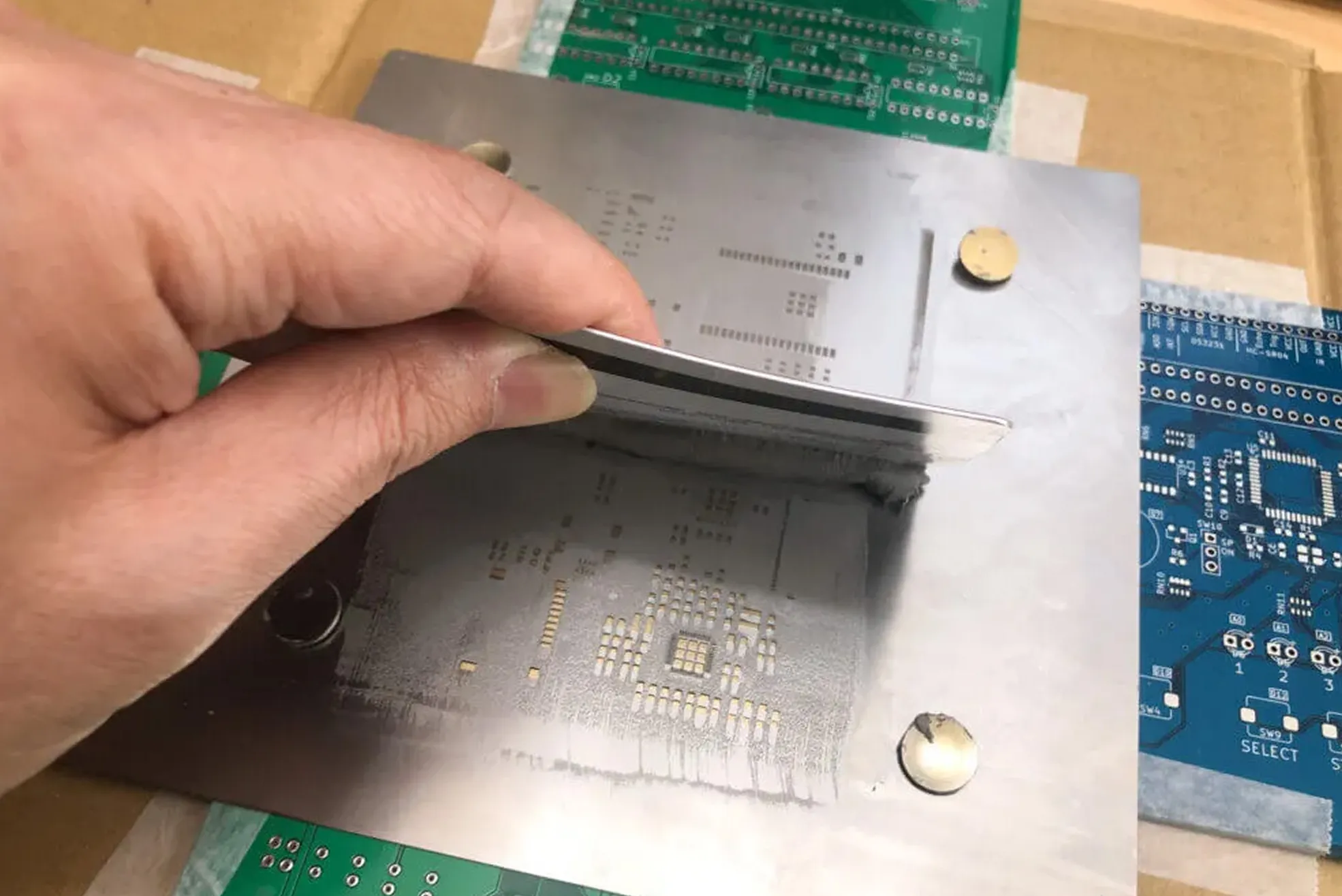
Step 4: Test the Stencil Fit
Place the finished stencil over your PCB to ensure the apertures align perfectly with the pads. Misalignment can lead to solder paste being applied in the wrong areas, causing assembly issues. Make adjustments if necessary by trimming or recutting specific areas. Once the fit is confirmed, your stencil is ready for use in manual SMT assembly stencil applications.
Best Practices for Solder Paste Application with a Stencil
With your stencil ready, the next step is mastering solder paste application. Proper technique is essential to avoid defects and ensure reliable soldering. Here are some tips to follow during the process.
Prepare Your Workspace and Materials
Work in a clean, well-lit area to avoid contamination of the solder paste or PCB. Gather the following:
- Solder paste (ensure it’s fresh and stored at the correct temperature, typically 2-10°C before use).
- A squeegee or plastic card to spread the paste.
- Isopropyl alcohol and lint-free wipes for cleaning.
- Your PCB and stencil.
Allow the solder paste to reach room temperature (around 25°C) for about 1-2 hours before use to ensure smooth application. Secure the PCB to your workspace with tape or a holder to prevent movement during paste application.
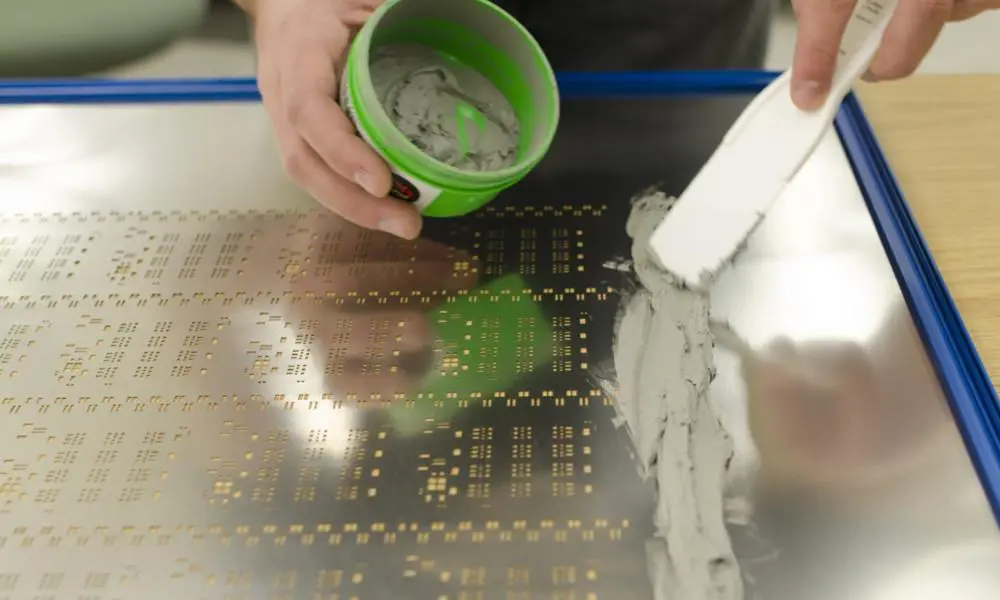
Align and Secure the Stencil
Place the stencil over the PCB, ensuring the apertures align perfectly with the pads. Use masking tape or small clamps to hold the stencil in place. For manual assembly, fiducial marks (if included in your design) can help with alignment, though they are more critical in automated processes.
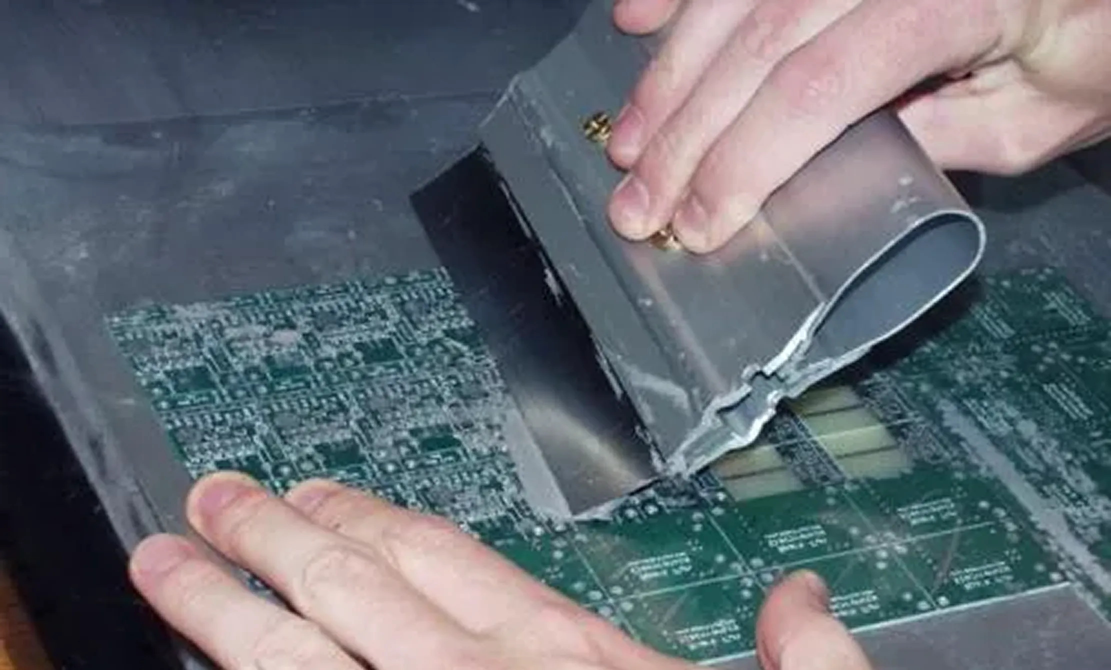
Apply the Solder Paste
Place a small amount of solder paste (about a 1-2 cm line) along one edge of the stencil. Using a squeegee or plastic card at a 45-degree angle, spread the paste across the stencil with steady, even pressure. Make one or two passes to ensure the paste fills all apertures. Avoid applying too much pressure, as this can cause paste to seep under the stencil and create smears.
After spreading, carefully lift the stencil straight up to avoid smudging the paste. Inspect the PCB for even deposits. If you notice gaps or uneven areas, clean the board with isopropyl alcohol, realign the stencil, and try again.
Clean the Stencil After Use
Immediately after use, clean the stencil with isopropyl alcohol and a lint-free wipe to remove excess solder paste. Dried paste can clog apertures and affect future applications. Store the stencil flat in a protective cover to prevent damage.
Optimizing Stencil Design for SMT Success
A well-thought-out stencil design for SMT can make a significant difference in the quality of your assembly. Here are some design considerations to keep in mind:
- Aperture Size: For fine-pitch components (pads closer than 0.5 mm), reduce aperture size by 10-20% to prevent solder bridging. For larger components, keep apertures closer to the pad size for adequate paste volume.
- Stencil Thickness: Use a 0.1 mm thick stencil for components with pitches below 0.5 mm and a 0.15 mm stencil for larger components to balance paste volume.
- Material Durability: Stainless steel lasts longer and provides better precision than Mylar, especially for repeated use. However, Mylar is more affordable and easier to cut for one-off projects.
Testing and adjusting your design based on trial runs can help fine-tune the stencil for your specific components and PCB layout.
Common Challenges and How to Overcome Them
Even with careful preparation, challenges can arise during solder paste application or stencil creation. Here are some common issues and solutions:
- Uneven Paste Deposits: This often results from inconsistent squeegee pressure or a poorly aligned stencil. Apply steady pressure and double-check alignment before starting.
- Solder Bridging: Excess paste can cause bridges between pads, especially with fine-pitch components. Use a thinner stencil or reduce aperture size to control paste volume.
- Stencil Misalignment: If the stencil shifts during application, secure it more firmly with tape or clamps. Adding reference marks on the PCB and stencil can also help with alignment.
Benefits of DIY Stencils for Small-Scale Projects
Opting for a solder paste stencil DIY approach offers several advantages for hobbyists and small-scale producers:
- Cost-Effective: Professional stencil fabrication can cost $50 or more, while DIY options using affordable materials like Mylar cost just a few dollars.
- Customization: You can tailor the stencil to your exact needs, adjusting aperture sizes or thickness based on trial and error.
- Learning Opportunity: Creating your own stencil provides hands-on experience with SMT processes, helping you better understand assembly challenges.
Final Thoughts on Manual SMT Assembly Stencils
Creating a manual SMT assembly stencil is a rewarding process that empowers you to take control of your PCB assembly projects. By following the steps outlined in this guide, from PCB stencil making to mastering solder paste application, you can achieve professional-quality results without the high costs of automated equipment. A well-designed stencil, paired with careful technique, ensures precise solder paste placement, leading to reliable soldering and functional circuits.
Whether you’re building prototypes or small production runs, investing time in stencil design for SMT pays off with improved efficiency and fewer defects. Start with simple materials and tools, refine your process through practice, and enjoy the satisfaction of assembling your own surface-mount PCBs with precision.