 ALLPCB


Introduction
BGA rework presents unique difficulties for electrical engineers who must restore functionality to assembled boards without introducing new defects. Engineers frequently encounter situations where conventional soldering techniques fall short because of the hidden nature of BGA connections. Successful rework requires precise control over temperature, alignment, and material handling to maintain long-term reliability. The process becomes especially demanding when boards contain high-density components or operate in environments with strict thermal cycling requirements. Understanding the most common BGA rework challenges allows teams to develop consistent procedures that reduce failure rates and extend product life.
What Is BGA Rework and Why It Matters
BGA rework involves the removal and replacement of ball grid array packages on populated printed circuit boards. This operation is essential in manufacturing environments where component failures occur after initial assembly or during field returns. Engineers rely on controlled heating, flux application, and precise placement to restore electrical and mechanical integrity. The technique supports both prototype debugging and high-volume repair lines where scrapping entire assemblies is not economical. Proper execution of BGA rework directly influences product reliability, warranty costs, and overall manufacturing yield.
Challenge 1: Controlling Thermal Profiles During Reflow
Uneven heating during BGA removal and replacement can damage adjacent components or the substrate itself. Engineers must balance peak temperatures high enough to melt solder balls while avoiding overheating of the board or package. Rapid temperature changes often create thermal gradients that stress solder joints and laminate materials. Without accurate profiling, boards may exhibit delamination or lifted pads after the rework cycle completes.
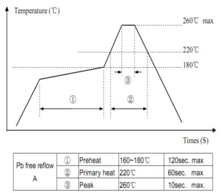
Industry standards such as IPC-7711/7721B provide guidance on establishing repeatable thermal profiles for surface-mount rework. Engineers typically use multiple thermocouples attached to the board and package to monitor actual temperatures at critical locations. Slow ramp rates and extended soak zones help equalize heat distribution across the assembly. Post-rework inspection with X-ray imaging confirms that solder joints have reached proper reflow without exceeding component ratings.
Challenge 2: Managing PCB and Component Warpage
Warpage of the printed circuit board or the BGA package itself disrupts uniform contact between solder balls and pads. This distortion often appears during the heating phase when different materials expand at unequal rates. Engineers observe that even minor warpage can prevent complete solder coalescence and create open circuits after cooling. Warpage becomes more pronounced on larger boards or those with asymmetric copper distribution.
Practical solutions include preheating the entire assembly to reduce thermal shock and using specialized fixtures that apply gentle pressure during reflow. Engineers also select rework stations equipped with bottom-side heating to minimize top-to-bottom temperature differences. Following established procedures from IPC-A-610G helps verify that warpage remains within acceptable limits before and after the operation.
Challenge 3: Achieving Precise Component Alignment
Accurate placement of the replacement BGA is critical because the solder balls are hidden beneath the package. Even small offsets can result in partial connections or bridging between adjacent balls. Engineers rely on optical systems or split-vision alignment tools to position the component relative to the pad pattern. Manual placement without magnification frequently leads to misalignment that only becomes evident after electrical testing.
Best practices include using flux that provides temporary tackiness to hold the package in position during transfer. Engineers also verify pad condition and apply fresh solder paste or flux dots when necessary. Consistent use of alignment verification steps reduces placement errors and improves first-pass success rates.
Challenge 4: Preventing Solder Joint Defects
Solder bridging, insufficient wetting, and void formation remain frequent outcomes when BGA rework parameters are not optimized. Bridging occurs when excess solder flows between adjacent balls during reflow. Insufficient solder volume or poor flux activity can leave open joints that fail under mechanical stress. Voids trapped inside the joint reduce thermal and electrical performance over time.
Engineers address these issues by selecting flux formulations compatible with the existing solder alloy and by controlling the amount of solder paste applied. X-ray inspection immediately after reflow reveals bridging or voids so corrective action can be taken before the board proceeds to testing. Maintaining clean work surfaces and using nitrogen atmospheres during reflow further minimizes oxidation-related defects.
Related Reading: Troubleshooting Common BGA Rework Defects: A Practical Guide
Challenge 5: Handling Moisture Sensitivity
BGA packages classified as moisture sensitive can absorb humidity that turns to steam during rapid heating, causing internal cracking or delamination. This phenomenon, often called popcorning, permanently damages the component and may propagate to the board. Engineers must identify the moisture sensitivity level of each package before rework begins.
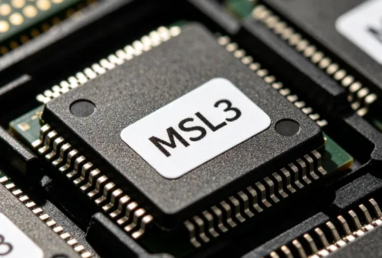
Following JEDEC J-STD-020E classification guidelines ensures proper baking procedures are applied when required. Components are stored in dry cabinets or baked at specified temperatures and durations prior to rework. This controlled handling prevents moisture-related failures and maintains the mechanical integrity of the reworked assembly.
Related Reading: BGA Rework for Beginners: A Hobbyist's Guide to Repairing Electronics
Conclusion
BGA rework challenges stem from the combination of hidden connections, thermal sensitivity, and strict alignment requirements. Engineers who apply structured thermal profiling, warpage mitigation, precise placement techniques, defect prevention methods, and moisture control achieve higher success rates. Consistent adherence to recognized industry standards supports repeatable results across different board designs and production volumes. These practices ultimately reduce scrap, shorten repair cycles, and improve overall product reliability.
FAQs
Q1: What are the most common BGA rework challenges engineers face?
A1: The primary BGA rework challenges include thermal profile control, PCB and package warpage, alignment accuracy, solder joint defects, and moisture sensitivity management. Each issue requires specific equipment settings and process controls to avoid introducing new failures during repair. Engineers address these systematically by monitoring temperatures, using alignment tools, and following moisture handling protocols.
Q2: How can BGA rework defects be minimized during the process?
A2: BGA rework defects are minimized through accurate thermal profiling, proper flux selection, and post-reflow X-ray inspection. Engineers also verify component moisture levels and maintain clean work environments to reduce bridging, voids, and opens. Consistent application of these steps improves joint quality and long-term reliability.
Q3: What solutions exist for common BGA rework issues?
A3: Solutions for BGA rework issues center on controlled heating, mechanical fixturing to counteract warpage, and optical alignment systems. Engineers combine these techniques with appropriate flux and solder volumes to achieve reliable connections. Regular process validation against industry standards further reduces the occurrence of defects.
Q4: Why is moisture sensitivity important in BGA rework?
A4: Moisture sensitivity matters because absorbed humidity can vaporize during reflow and damage the BGA package or surrounding board areas. Engineers follow established classification guidelines to determine baking requirements before rework. Proper handling prevents popcorning and ensures the reworked assembly meets original reliability expectations.
References
IPC-7711/7721B: Rework, Modification and Repair of Electronic Assemblies.
IPC-A-610G: Acceptability of Electronic Assemblies.
JEDEC J-STD-020E: Moisture/Reflow Sensitivity Classification for Nonhermetic Surface Mount Devices.


