 ALLPCB


Why Thermal Management Matters in Wearable Devices
Wearable electronics continue to shrink in size while adding more sensors, processors, and wireless modules. This miniaturization creates concentrated heat sources within tight enclosures that sit directly against the skin. Effective thermal management therefore becomes essential to maintain device performance and prevent user discomfort. Engineers must balance power density with the physical constraints of flexible substrates and curved surfaces. Heat paths in these designs often rely on conduction through thin layers rather than traditional airflow.
Compact form factors limit the space available for heat spreading and dissipation. Elevated temperatures can reduce battery life, trigger thermal throttling in processors, and degrade sensor accuracy. Prolonged skin contact also raises safety concerns if surface temperatures exceed comfortable limits. Industry standards such as IPC-2221 guide the layout of conductive traces and planes that serve as primary heat conductors in these assemblies. Proper thermal design therefore supports both reliability and user acceptance across medical, fitness, and consumer applications.
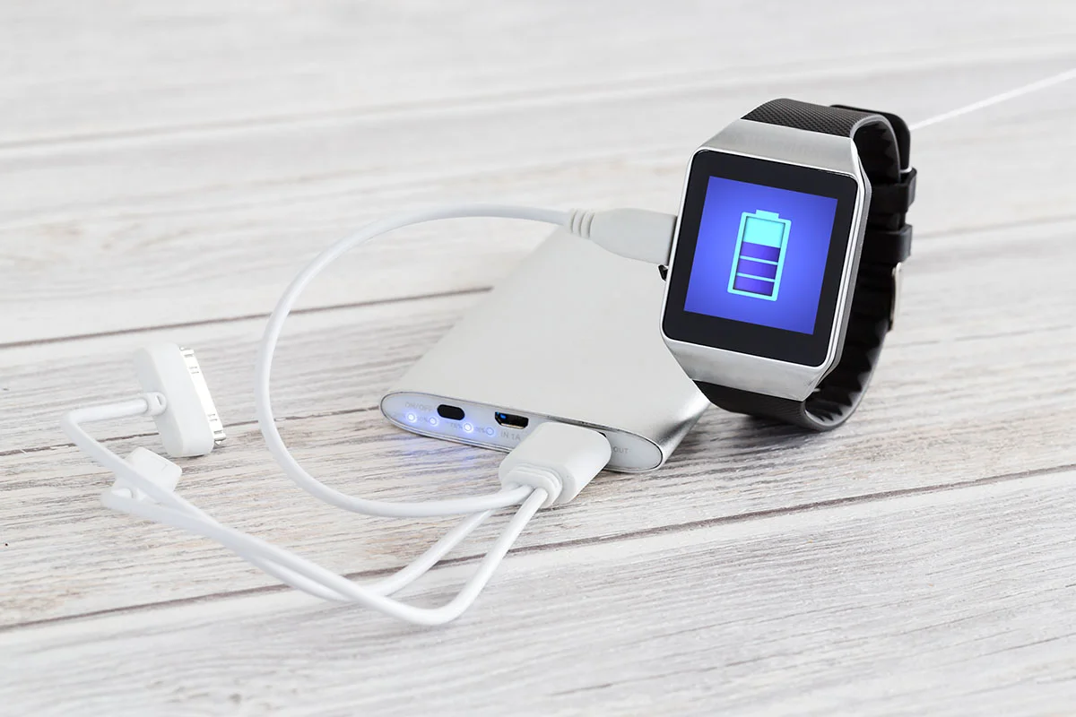
Engineering Mechanisms of Heat Transfer in Small Enclosures
Heat generated by active components travels primarily through conduction along copper layers and thermal interface materials. In flexible circuits the thin dielectric substrates offer limited lateral spreading, so localized hot spots form quickly. Convection plays a minor role because enclosures lack ventilation and natural airflow is blocked by body contact. Radiation contributes modestly at the low temperature differentials typical of wearables. Designers therefore focus on increasing effective thermal conductivity within the available volume while respecting bending requirements.
Low-profile thermal interface materials fill microscopic gaps between dies and heat spreaders without adding significant thickness. These materials must remain compliant during repeated flexing yet maintain stable contact resistance over the product lifetime. Flexible heat spreaders made from graphite or thin metal foils extend the heat path across larger areas before it reaches the outer surface. Body-worn cooling solutions such as phase-change layers or micro-channel structures can absorb transient peaks, but they add complexity to assembly and reliability testing.
Design Practices for Effective Heat Dissipation
Begin layout by identifying the highest-power components and mapping their thermal resistance paths to the enclosure exterior. Place high-conductivity planes directly beneath heat sources and connect them with thermal vias where substrate thickness permits. Keep trace routing dense enough to carry heat yet sparse enough to preserve flexibility. Select low-profile thermal interface materials with appropriate compressibility to accommodate tolerance stack-ups in curved housings.
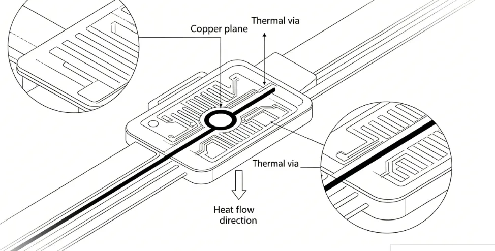
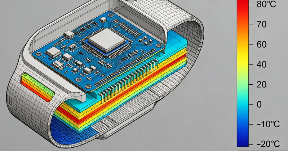
Verify the complete stack-up against IPC-6012E performance requirements for thermal and mechanical stability. Simulate steady-state and transient conditions early in the design cycle to predict skin-contact temperatures. Iterate component placement and material choices until maximum surface temperatures remain within acceptable limits for continuous wear. This structured approach reduces late-stage redesigns and supports consistent manufacturing yields.
Practical Implementation Considerations
During assembly, apply thermal interface materials uniformly to avoid air pockets that increase resistance. Align flexible heat spreaders precisely with heat-generating areas while allowing sufficient clearance for bending radii. Test completed modules under realistic use conditions that include body heat, motion, and varying ambient temperatures. Monitor both internal junction temperatures and external surface temperatures to confirm compliance with safety guidelines.
Conclusion
Thermal management in wearable electronics requires deliberate attention to conduction paths, material selection, and enclosure geometry. By following established design rules and verifying performance through simulation and testing, engineers can achieve reliable operation within shrinking form factors. The result is longer device life, improved user comfort, and broader adoption of advanced wearable technology.
FAQs
Q1: How do flexible heat spreaders improve heat dissipation in small enclosures?
A1: Flexible heat spreaders distribute heat laterally across thin, bendable layers, reducing localized hot spots in compact wearable designs. They integrate with existing PCB copper planes without adding bulk, supporting both thermal performance and mechanical flexibility required for body-worn applications.
Q2: What role do low-profile thermal interface materials play in wearable electronics?
A2: Low-profile thermal interface materials bridge microscopic gaps between components and heat spreaders while maintaining minimal thickness. Their compliance ensures consistent contact during flexing and repeated use, directly contributing to lower operating temperatures in space-constrained enclosures.
Q3: Why is heat dissipation in small enclosures critical for body-worn cooling solutions?
A3: Limited volume restricts natural convection, so heat must conduct efficiently to the outer surface for dissipation. Effective body-worn cooling solutions rely on optimized paths through the PCB and enclosure to keep skin-contact temperatures comfortable and maintain device reliability over extended wear periods.
Q4: How can engineers verify thermal performance without physical prototypes?
A4: Finite-element thermal simulation combined with material property data allows early evaluation of temperature distributions. Results are then validated against IPC-6012E acceptance criteria during subsequent prototype testing to confirm compliance before volume production.
References
IPC-2221 — Generic Standard on Printed Board Design. IPC, 2023
IPC-6012E — Qualification and Performance Specification for Rigid Printed Boards. IPC, 2017
JEDEC J-STD-020E — Moisture/Reflow Sensitivity Classification. JEDEC, 2014





