 ALLPCB


Introduction
In high-speed PCB design, maintaining signal integrity is crucial as data rates continue to increase, demanding precise control over electrical performance. Microvias, essential for high-density interconnect (HDI) structures, enable compact layouts by providing short vertical connections between layers. However, their introduction can influence microvia signal integrity through effects on impedance, crosstalk, and reflections. Engineers must understand these interactions to optimize performance in applications like telecommunications and computing. This article explores the mechanisms behind these impacts and offers structured guidance for effective implementation. By aligning microvia usage with established design principles, high-speed PCBs can achieve reliable operation.
What Are Microvias and Why They Matter in High-Speed PCB Design
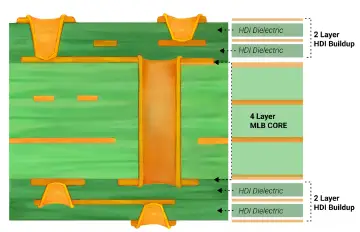
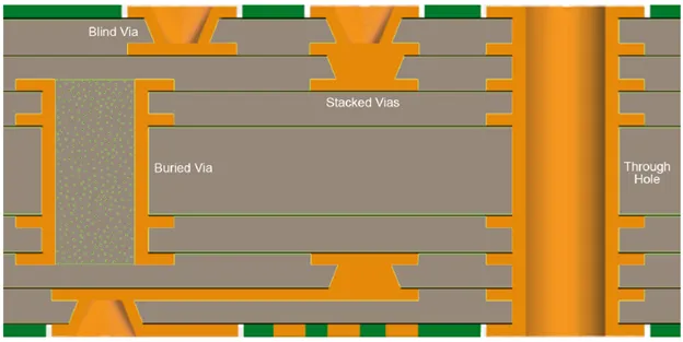
Microvias are small-diameter vias, typically laser-drilled with diameters of 150 micrometers or less, connecting only adjacent layers in multilayer boards. They form the backbone of HDI PCBs, allowing for finer pitch components and increased routing density compared to traditional through-vias. In high-speed PCB design, microvias shorten signal paths, reducing propagation delays and parasitic effects that degrade performance. Their staggered or stacked configurations support complex stackups, but require careful planning to preserve microvia signal integrity. As board densities rise, microvias become indispensable for accommodating ball grid arrays with pitches below 0.8 millimeters. Ultimately, their role extends beyond density to directly affecting electrical characteristics like return path continuity.
The relevance of microvias stems from the shift toward faster interfaces operating in the multi-gigabit range. Longer conventional vias introduce stubs that resonate at high frequencies, causing insertion loss and reflections. Microvias mitigate these by eliminating unnecessary stub lengths, promoting cleaner signal transmission. They also facilitate thinner dielectrics, which enhance coupling between signals and reference planes. For electrical engineers, mastering microvia integration ensures compliance with performance margins in demanding environments. Proper deployment translates to lower bit error rates and improved overall system reliability.
Technical Principles: Mechanisms Affecting Microvia Signal Integrity
Microvia Impedance Control
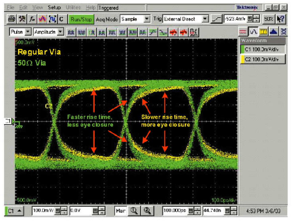
Microvia impedance arises from transitions between traces and vias, where geometry changes can create discontinuities. The small size of microvias reduces inductance compared to larger vias, but plating quality and fill uniformity are critical to avoid voids that alter local impedance. Thin dielectrics in HDI stackups tighten signal-to-reference coupling, aiding consistent characteristic impedance along the path. In high-speed designs, mismatches lead to ringing and eye closure, compromising data integrity. Engineers model these transitions to predict and compensate for variations during layout. Adhering to guidelines like those in IPC-2226 helps maintain controlled microvia impedance across frequencies.
Stacking multiple microvias amplifies cumulative effects, as each transition adds potential mismatch. Aspect ratios below 0.8:1 ensure reliable plating, minimizing resistance spikes. Reference plane changes during layer transitions further challenge impedance if not addressed with stitching. Simulations reveal how dielectric thickness influences distributed capacitance, stabilizing impedance profiles. For differential pairs, symmetric microvia placement prevents skew-induced imbalances. Thus, impedance control demands holistic stackup planning from the outset.
Microvia Crosstalk
Crosstalk in microvias occurs through capacitive and inductive coupling between adjacent structures, exacerbated by dense routing. Shorter microvia lengths reduce coupled path durations, inherently lowering far-end and near-end crosstalk compared to through-vias. Guard traces or ground stitching between high-speed lines further shields signals, diverting coupled noise to low-impedance returns. Thin dielectrics enhance reference plane effectiveness, suppressing mutual inductance between traces. In HDI boards, orthogonal routing on adjacent layers minimizes parallel run lengths that amplify coupling. Overall, microvia designs can outperform traditional vias when spacing and shielding are optimized.
High-density environments test these principles, as microvia clusters near components increase proximity risks. Differential signaling leverages common-mode rejection to cancel induced noise effectively. Solid ground planes beneath signal layers provide return paths that absorb crosstalk currents. Engineers quantify coupling via field solvers to set spacing rules. Staggered microvias distribute stress and coupling more evenly than stacked ones. These mechanisms ensure microvia crosstalk remains manageable in high-speed PCB design.
Microvia Reflections
Reflections from microvias stem primarily from impedance discontinuities and stub resonances in mismatched structures. By limiting connections to adjacent layers, microvias avoid long stubs that reflect energy at quarter-wave frequencies. Positioning microvias close to pads minimizes trace stubs, reducing reflection coefficients. Sequential transitions require via-in-pad techniques to smooth the path. Return path disruptions during plane changes can induce reflections if stitching is inadequate. Proper design keeps reflections below thresholds that close signal eyes.
In stacked configurations, accumulated transitions heighten reflection risks without copper filling for planarity. Laser-drilled precision aids clean geometries, but plating uniformity prevents barrel cracks that scatter signals. Thermal vias nearby manage heat without introducing additional discontinuities. Simulations validate reflection mitigation by overlaying S-parameters. For high-speed signals, eliminating stubs preserves waveform fidelity. Thus, microvia reflections are controllable through geometry and layout discipline.
Best Practices for Microvia Design in High-Speed PCBs
Selecting low dielectric constant and low dissipation factor materials forms the foundation for microvia signal integrity. These reduce propagation delays and attenuation, supporting clean high-frequency transmission. Stackups with signal layers sandwiched between ground planes ensure low-impedance returns and EMI shielding. Orthogonal routing and symmetric builds prevent warping that misaligns vias. Per IPC-2226, classify HDI types to match complexity, favoring staggered vias for reliability.
Position microvias adjacent to signal pads using via-in-pad technology to eliminate stubs and reflections. Decoupling capacitors near power pins stabilize supplies, indirectly aiding signal stability. Guard traces and stitching vias between lines suppress microvia crosstalk. Maintain equal trace lengths for clocks to avoid skew. Thermal vias dissipate heat without compromising paths.
Reference plane transitions demand co-located ground stitching, especially for differential pairs in patterns like ground-signal-ground. Avoid plane splits under high-speed areas to preserve continuity. Simulate return paths to identify inductance hotspots. Aspect ratios per IPC-T-50M guidelines ensure plating integrity, reducing failures that degrade performance. These practices collectively enhance microvia impedance and overall integrity.
Troubleshooting Insights for Microvia-Related Signal Issues
Engineers often encounter elevated insertion loss from stacked microvias due to sequential transitions. Verify fill quality and dielectric homogeneity to rule out voids. Crosstalk spikes near BGA escapes signal inadequate spacing or missing guards. Review simulations against measurements for correlation. Reflections persisting post-optimization point to return path discontinuities, addressed by denser stitching. Reliability testing per IPC methods confirms thermal stability without cracks.
Conclusion
Microvias profoundly shape signal integrity in high-speed PCB design by enabling density while introducing impedance, crosstalk, and reflection challenges. Shorter paths and stub elimination offer advantages, but demand precise control through materials, stackups, and stitching. Best practices like those aligned with IPC standards ensure robust performance. Electrical engineers benefit from structured analysis and simulation to balance trade-offs. Implementing these principles yields PCBs ready for multi-gigabit demands. Future designs will lean further on optimized microvias for advancing speeds.
FAQs
Q1: What is microvia signal integrity in high-speed PCB design?
A1: Microvia signal integrity refers to preserving electrical signal quality through microvia structures, addressing impedance mismatches, crosstalk, and reflections. Short vias reduce parasitics, but transitions require stitching for return paths. Low-Dk materials and symmetric layouts maintain waveform fidelity. Following IPC-2226 guidelines supports reliable HDI implementations. This ensures data rates without degradation.
Q2: How does microvia impedance affect high-speed signals?
A2: Microvia impedance discontinuities arise at trace-to-via junctions, potentially causing ringing if uncontrolled. Thin dielectrics enhance coupling for stability. Stacked vias accumulate mismatches without proper filling. Simulations predict profiles for compensation. Optimized designs keep variations minimal, preserving eye opening.
Q3: What causes microvia crosstalk and how to mitigate it?
A3: Microvia crosstalk results from coupling in dense arrays, reduced by short lengths and guards. Ground planes absorb noise via low-impedance returns. Orthogonal routing limits parallel runs. Differential pairs cancel common-mode interference. Stitching enhances shielding effectiveness.
Q4: How to minimize microvia reflections in PCB layouts?
A4: Place microvias near pads to shorten stubs, eliminating resonances. Via-in-pad caps smooth transitions. Stitching maintains returns during plane changes. Avoid asymmetries in pairs. These steps keep reflections low for clean signals.


