 ALLPCB


Introduction
Printed circuit board reliability remains a central concern for electrical engineers working on systems exposed to mechanical shock, vibration, and repeated thermal cycling. Traditional surface-mount assemblies rely heavily on solder joints that can crack or fatigue over time, leading to intermittent or complete failures. Embedded components address these issues by integrating passive devices directly into the PCB substrate layers. This approach reduces the number of exposed solder joints while improving overall mechanical and thermal stability. Engineers increasingly evaluate embedded technology when designing for extended service life in demanding environments.
Why Embedded Components Matter for PCB Reliability
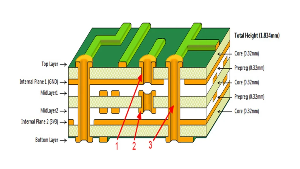
Embedded components place resistors, capacitors, and sometimes inductors within the inner layers of the board rather than on the outer surfaces. This configuration eliminates many solder joints that would otherwise serve as primary failure points under mechanical stress. The result is enhanced vibration resistance PCB performance because the components experience less relative movement during flexure or shock events. Thermal stress PCB management also improves since the embedded devices share the same coefficient of thermal expansion as the surrounding laminate material. Over the product lifetime, these changes contribute to higher component lifetime expectations in applications ranging from automotive electronics to industrial controls.
Technical Principles of Embedded Component Integration
The core engineering advantage lies in the elimination of discrete solder connections for passive elements. Each removed joint removes a potential site for crack initiation caused by coefficient of thermal expansion mismatch during temperature excursions. When components reside inside the dielectric layers, mechanical loads from board flexure distribute more evenly across the surrounding material instead of concentrating at joint interfaces. This distribution directly supports improved vibration resistance PCB characteristics, as the embedded devices move in unison with the board rather than acting as separate masses attached by compliant solder. Thermal cycling reliability benefits similarly because heat paths become more uniform and expansion stresses remain internal to the composite structure.
Industry standards such as IPC-6012E provide qualification requirements that help ensure the integrity of both surface and embedded features in rigid boards. Manufacturing processes must maintain precise registration and void-free lamination to realize these reliability gains. Engineers therefore review stack-up designs and material selections early to confirm compatibility with embedding techniques.
Related Reading: Embedded Components in PCB Design: Innovations and Use Cases
Mechanisms Reducing Thermal Stress and Extending Component Lifetime
Thermal stress PCB arises primarily from repeated expansion and contraction cycles that strain solder joints. Embedding passive components moves those devices away from the highest-stress surface regions and into a more constrained internal environment. The surrounding laminate constrains movement, reducing strain on the component terminations. This constraint helps maintain electrical performance over longer periods, supporting extended component lifetime in temperature-cycled applications. In addition, the absence of surface-mounted parts in certain areas allows for more consistent copper distribution, which further moderates local temperature gradients during operation.
Vibration resistance PCB improvements follow a similar logic. Surface-mounted components can resonate at frequencies that accelerate fatigue at their solder fillets. Embedded parts lack these external attachment points and therefore exhibit higher natural frequencies or damped responses within the board structure. Design teams quantify these effects through modal analysis and accelerated life testing aligned with relevant IPC and JEDEC guidelines.
Practical Design and Manufacturing Considerations
Engineers begin by identifying which passive values can be embedded without compromising routing density or signal integrity. Capacitance and resistance values are realized through patterned conductive layers or filled vias within the core materials. Layout tools must account for the different tolerances associated with embedded fabrication compared with discrete parts. Close collaboration between design and fabrication teams ensures that drill and lamination processes meet the positional accuracy needed for reliable performance.
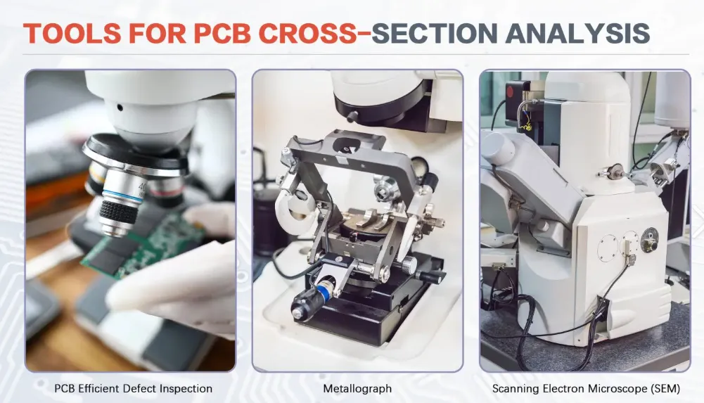
Process controls during lamination and curing directly influence the final reliability. Proper pressure and temperature profiles prevent delamination around embedded features. Post-lamination inspection, including cross-section analysis, verifies that components remain intact and properly encapsulated. These steps align with the performance criteria outlined in standards such as IPC-A-600K for board acceptability.
Related Reading: The Essential Guide to Embedded Component PCB Design Software
Best Practices for Maximizing Durability Gains
Select laminate systems with glass transition temperatures and expansion characteristics compatible with the embedded components and expected operating conditions. Maintain balanced copper distribution on inner layers to minimize warpage that could induce additional stress. When surface-mount components remain necessary, position them away from high-flexure zones and use underfill or staking where vibration levels are extreme. Document all material and process parameters so that subsequent builds maintain the reliability improvements achieved in the initial design.
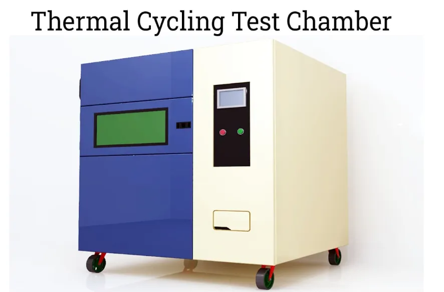
Testing protocols should include both thermal cycling and random vibration profiles representative of the end-use environment. Results from these tests guide iterative refinements to stack-up or component placement. Following established industry standards throughout the development cycle helps ensure consistent outcomes across production lots.
Conclusion
Embedded components offer electrical engineers a practical method to enhance PCB reliability by reducing solder joint count and improving resistance to vibration and thermal stress. The resulting designs exhibit longer component lifetime under demanding conditions while maintaining electrical functionality. Successful implementation requires attention to material selection, process controls, and verification testing aligned with recognized industry standards. When applied thoughtfully, this technology supports more robust electronic systems across multiple sectors.
FAQs
Q1: What are embedded components in PCBs and how do they affect reliability?
A1: Embedded components integrate passive devices within the board layers instead of mounting them on the surface. This reduces the number of solder joints, which are common failure sites under mechanical and thermal loads, thereby improving overall PCB reliability and extending component lifetime.
Q2: How do embedded components improve vibration resistance PCB performance?
A2: By placing components inside the substrate, relative motion between the device and the board is minimized during flexure or shock. The integrated structure distributes mechanical energy more evenly, reducing fatigue at attachment points and enhancing vibration resistance PCB characteristics.
Q3: Can embedded components reduce thermal stress PCB issues?
A3: Yes. Embedding moves passive elements into a more uniform thermal environment where expansion is constrained by the surrounding laminate. This reduces differential strain on terminations and helps maintain performance through repeated temperature cycles.
Q4: What standards guide the use of embedded components for durability?
A4: Qualification and acceptability requirements appear in documents such as IPC-6012E and IPC-A-600K. These standards address the fabrication and inspection criteria needed to achieve reliable embedded structures.





