ALLPCB


Introduction
PCB gold finger plating plays a critical role in ensuring reliable electrical connections for edge connectors in applications ranging from consumer electronics to high-reliability systems. These gold-plated segments on printed circuit board edges provide excellent conductivity, corrosion resistance, and durability under repeated insertions. However, the traditional electroplating processes involved generate significant environmental concerns, including hazardous chemical waste and heavy metal contamination. As regulatory pressures mount and sustainability becomes a core factory priority, manufacturers must adopt practices that minimize ecological footprints while maintaining performance standards. This article explores the environmental impacts of gold finger plating and outlines sustainable manufacturing approaches, such as environmentally friendly gold plating and wastewater treatment for gold plating. Factory-driven insights reveal how these strategies align with industry demands for RoHS compliance for gold fingers and overall sustainable PCB manufacturing.
What Are PCB Gold Fingers and Why Do They Matter for Sustainability?
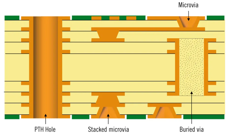
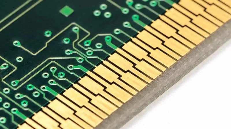
Gold fingers refer to the gold-plated contact pads along the edge of a PCB designed for insertion into card slots or connectors. Typically, they consist of a nickel underlayer electroplated with a thin hard gold finish to withstand mechanical wear and ensure low contact resistance. This plating is essential for high-cycle applications like graphics cards or backplanes where reliability directly impacts system performance. From a sustainability perspective, gold fingers matter because their production consumes precious metals and generates process waste that can harm ecosystems if not managed properly. The global demand for PCBs amplifies these issues, as e-waste from discarded boards contains recoverable gold, underscoring the need for closed-loop practices. Factories focusing on reducing waste in gold plating can achieve cost savings alongside environmental benefits.
Technical Principles Behind Gold Finger Plating and Its Environmental Footprint
The standard gold finger plating process begins with surface preparation, followed by electroless or electrolytic nickel deposition, and culminates in electroplating a gold layer, often 0.75 to 2.5 micrometers thick depending on requirements. Traditional baths employ cyanide-based electrolytes for gold deposition, which offer high efficiency but pose severe toxicity risks due to cyanide's potential to release hydrogen cyanide gas or contaminate water sources. Rinse waters from these steps carry dissolved metals like gold, nickel, and copper, leading to wastewater laden with heavy metals that bioaccumulate in aquatic life. Energy-intensive electrolytic processes further contribute to the carbon footprint through high power consumption in plating tanks. Poorly controlled plating can result in defects like porosity or uneven coverage, increasing scrap rates and waste. These mechanisms highlight why sustainable PCB manufacturing must target both process chemistry and waste streams.
Key Environmental Impacts of Traditional Gold Finger Plating
Traditional gold plating releases hazardous effluents that challenge wastewater treatment capabilities in PCB factories. Cyanide and acid-based solutions can leach into soil and water if spills occur, while metal-laden sludge from treatment processes requires specialized disposal. The mining and refining of gold for plating contribute upstream impacts, including habitat destruction and high water usage, though downstream manufacturing controls offer immediate mitigation opportunities. Discarded PCBs with gold fingers add to e-waste piles, where unrecovered gold perpetuates resource depletion. Energy use in maintaining plating bath temperatures and agitation systems adds to greenhouse gas emissions. Collectively, these impacts drive the industry toward practices like recycling gold from PCBs to close material loops and reduce virgin resource demands.
Sustainable Practices: Environmentally Friendly Gold Plating Techniques
Transitioning to environmentally friendly gold plating involves replacing cyanide with non-toxic alternatives like thiosulfate or sulfite-based electrolytes, which maintain plating efficiency without the risks of lethal byproducts. These formulations enable factories to deposit uniform gold layers suitable for gold fingers while simplifying downstream treatment. Selective plating, where gold is applied only to finger areas via masking, minimizes material usage and waste generation. Optimizing plating thickness per application needs, guided by standards like IPC-4556, further reduces gold consumption without compromising durability. Factories implementing these methods report lower chemical procurement costs and easier regulatory compliance. Such approaches form the foundation of sustainable PCB manufacturing by prioritizing precision over excess.
Reducing Waste in Gold Plating and Material Recovery Strategies
Reducing waste in gold plating starts with drag-out minimization through efficient rinsing protocols and bath drag reduction agents that limit metal carryover. Closed-loop systems recirculate rinse water after filtration, cutting freshwater intake and effluent volume. Gold recovery from spent baths and rinses employs electrowinning or ion exchange resins to precipitate metals for reuse, transforming waste into a resource. Factory scrap from edge trimming often contains viable gold fingers, which can be stripped and refined on-site or via certified partners. These strategies not only curb landfill contributions but also offset raw material expenses. Integrating them ensures long-term viability in resource-constrained environments.
Recycling Gold from PCBs: A Closed-Loop Approach
Recycling gold from PCBs targets end-of-life boards and manufacturing rejects, where gold fingers represent a concentrated source of the metal. Processes involve mechanical separation of fingers via shearing or depopulation, followed by chemical stripping using nitric acid or alkaline solutions to dissolve base metals while preserving gold. The recovered gold foils undergo further refining to 99.9% purity for replating reuse. Factories adopting this practice divert tons of e-waste annually, aligning with circular economy principles. Challenges like solder contamination require pre-treatments such as desoldering, but yields justify the effort. Recycling gold from PCBs thus supports sustainable PCB manufacturing by extending material lifecycles.
Wastewater Treatment for Gold Plating: Factory Best Practices
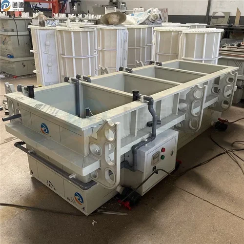
Effective wastewater treatment for gold plating employs multi-stage systems starting with pH adjustment to precipitate metals as hydroxides. Chemical reduction converts hexavalent chromium or cyanide to less toxic forms, while ion exchange selectively removes gold and nickel ions for recovery. Membrane filtration like ultrafiltration retains particulates, enabling water reuse in non-critical rinses. Advanced oxidation processes degrade organic additives, ensuring effluent meets discharge limits. Factories must monitor total dissolved solids and conduct regular sludge analysis to prevent secondary pollution. These treatments ensure compliance while enabling zero-liquid discharge goals.
RoHS Compliance for Gold Fingers and Regulatory Alignment
RoHS compliance for gold fingers focuses on eliminating restricted substances like lead in underlayers or fluxes during plating. Gold itself is RoHS-exempt, but nickel barriers must avoid cadmium or mercury impurities. Factories verify compliance through material certifications and process audits, often referencing IPC-6012 for qualification specs. Selective plating reduces exposure risks by limiting hazardous chemical zones. Integrating RoHS from design stage prevents rework and fines. This regulatory alignment bolsters sustainable credentials.
Best Practices for Implementing Sustainable Gold Finger Plating
Factories should conduct plating line audits to identify waste hotspots, then retrofit with cyanide-free chemistries and recovery units. Train operators on precise bath controls to avoid over-plating, adhering to IPC-A-600 acceptability criteria. Partner with recyclers for consistent gold reclaim streams, tracking recovery rates quarterly. Design PCBs for minimal gold area without sacrificing bevels or chamfers needed for insertion. Pilot selective plating on high-volume runs to validate performance. These steps embed sustainability into operations.
Insights from Factory Implementations
In high-volume PCB production, factories adopting gold recovery have recouped significant metal volumes from rinse streams alone. One insight reveals that combining ion exchange with electrowinning achieves over 95% gold recovery, though exact figures vary by bath chemistry. Challenges like inconsistent scrap quality demand robust preprocessing. Success hinges on cross-departmental buy-in, from design to quality control. These real-world shifts demonstrate scalable paths to sustainable PCB manufacturing.
Conclusion
Sustainable gold finger plating mitigates environmental impacts through cyanide-free processes, waste reduction, gold recycling, and advanced wastewater treatment. RoHS compliance reinforces these efforts, ensuring market access. Factories gain competitive edges via cost recoveries and regulatory alignment. As standards evolve, proactive adoption positions manufacturers as leaders in green electronics. Prioritizing these practices fosters resilient, eco-conscious supply chains.
FAQs
Q1: What are the main benefits of environmentally friendly gold plating for PCB gold fingers?
A1: Environmentally friendly gold plating uses non-cyanide electrolytes, reducing toxicity risks and simplifying wastewater treatment for gold plating. It maintains gold finger reliability for edge connectors while lowering chemical handling hazards. Factories achieve sustainable PCB manufacturing with easier compliance and potential material savings. This approach aligns with factory-driven standards for long-term viability.
Q2: How can factories reduce waste in gold plating processes?
A2: Reducing waste in gold plating involves selective application to gold fingers only, optimized rinse cycles, and closed-loop water systems. Recovery techniques like electrowinning reclaim gold from effluents, minimizing disposal needs. Adhering to process controls per industry standards prevents defects and scrap. These steps support efficient, low-impact operations.
Q3: Why is recycling gold from PCBs important for sustainability?
A3: Recycling gold from PCBs recovers valuable metal from end-of-life boards and factory scrap, reducing reliance on mining. Gold fingers provide high-concentration sources, enabling efficient stripping and refining. This practice cuts e-waste and promotes circular economies in sustainable PCB manufacturing. Factories benefit from cost offsets and environmental stewardship.
Q4: How does RoHS compliance affect gold finger plating?
A4: RoHS compliance for gold fingers ensures no restricted substances in plating layers or processes, focusing on lead-free underplates. Gold deposition remains unaffected, but verification through audits is essential. Factories integrate this during fabrication to meet global regulations. It enhances sustainable practices without performance trade-offs.
References
IPC-6012E — Qualification and Performance Specification for Rigid Printed Boards. IPC, 2017
IPC-4556 — Specification for Electroplated Au over Ni/Pd for Printed Boards. IPC, 2013
IPC-A-600K — Acceptability of Printed Boards. IPC, 2020