ALLPCB


Why Advanced DFM Matters in High-Speed HDI Designs
High-speed PCB design rules become essential once clock frequencies exceed several hundred megahertz or edge rates fall below one nanosecond. At these speeds, even small variations in trace width, dielectric thickness, or via placement can degrade performance. Signal integrity analysis performed early in the design cycle identifies potential issues before fabrication begins. Impedance control techniques and crosstalk minimization strategies must be integrated with manufacturing constraints to avoid costly respins. EMI reduction DFM practices further ensure compliance with regulatory limits without adding excessive shielding or filtering.
Technical Principles Behind Signal Integrity and Manufacturability
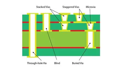
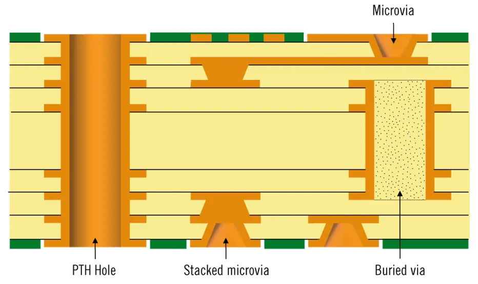
Signal propagation in high-speed digital circuits depends on consistent characteristic impedance along every transmission path. Variations arise from changes in trace geometry, copper thickness, or the surrounding dielectric materials. In HDI constructions, microvias and fine-line features introduce additional variables that affect return loss and insertion loss. Crosstalk occurs when electromagnetic fields from one trace couple into adjacent conductors, and its severity increases with faster edge rates and closer spacing. EMI reduction requires attention to current return paths, ground plane integrity, and the placement of decoupling structures. These mechanisms interact with fabrication tolerances, so DFM reviews evaluate both electrical targets and achievable process limits.
Manufacturing processes impose their own constraints on high-speed layouts. Etch factor, plating uniformity, and lamination pressure all influence final trace profiles and dielectric spacing. Thermal expansion differences between materials can create warpage that affects via registration and surface flatness. These physical effects directly impact the repeatability of impedance and the effectiveness of crosstalk control measures.
Practical DFM Solutions and Best Practices
Design teams begin by establishing clear high-speed PCB design rules that incorporate both electrical simulations and fabrication capabilities. Trace widths and spacings are chosen to meet target impedances while staying within the minimum feature sizes and aspect ratios supported by the chosen process. Differential pairs receive matched lengths and controlled spacing to preserve signal integrity. Via structures are optimized by selecting appropriate pad sizes, drill diameters, and fill methods that minimize stubs and maintain consistent impedance transitions.
Impedance control techniques include specifying stackup details such as dielectric constants, copper weights, and core thicknesses early in the project. Pre-layout modeling verifies that the proposed construction will achieve the required tolerances after accounting for typical process variations. Crosstalk minimization benefits from increased spacing between critical nets, the use of ground planes between signal layers, and routing strategies that avoid parallel runs over long distances. EMI reduction DFM incorporates continuous ground planes, strategic stitching vias, and careful component placement to shorten return current loops.
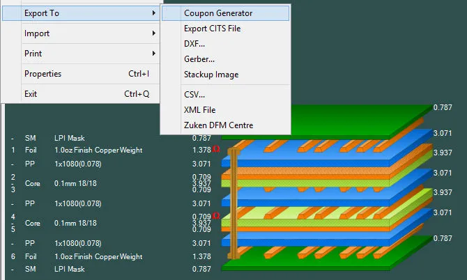
Layer stackup reviews conducted with manufacturing input help identify potential issues such as resin starvation around dense via fields or copper imbalance that leads to warpage. Design rules for via placement avoid clustering that exceeds drill registration tolerances. Surface finish selection considers both high-frequency skin effect and assembly requirements. These coordinated steps reduce the likelihood of performance shortfalls after boards are built.
Quality Alignment with Industry Standards
Design and fabrication practices align with established specifications that define acceptable performance and workmanship. IPC-6012E provides qualification and performance criteria for rigid printed boards, guiding material and construction choices that support high-speed applications. IPC-A-600K outlines visual and dimensional acceptance standards that help maintain consistency across production lots.
Conclusion
Advanced DFM techniques integrate electrical requirements with manufacturing realities to produce reliable high-speed digital HDI PCBs. Early attention to impedance control techniques, crosstalk minimization, and EMI reduction DFM practices, combined with thorough signal integrity analysis, improves both performance and yield. Structured reviews against documented standards further support consistent results across design iterations.
FAQs
Q1: How do high speed PCB design rules incorporate impedance control techniques?
A1: High speed PCB design rules define target impedance values along with allowable tolerances for trace width, spacing, and dielectric thickness. These rules are developed from stackup modeling that accounts for process variations. Designers then apply the rules during layout to maintain consistent characteristic impedance and minimize reflections.
Q2: What role does signal integrity analysis play in crosstalk minimization?
A2: Signal integrity analysis simulates coupling between adjacent traces under worst-case switching conditions. The results guide adjustments to spacing, layer assignment, and the insertion of ground planes or guard traces. This proactive approach reduces crosstalk before boards reach fabrication.
Q3: Which EMI reduction DFM practices are most effective for HDI boards?
A3: Effective EMI reduction DFM practices include maintaining continuous reference planes, using stitching vias to connect ground layers, and optimizing component placement to shorten current return paths. These measures are verified through both simulation and post-layout review to limit radiated and conducted emissions.
Q4: How do manufacturing tolerances affect impedance control techniques in high-speed designs?
A4: Manufacturing tolerances influence final trace geometry and dielectric spacing, which in turn shift actual impedance from the design target. DFM reviews compare simulated values against expected process variations and adjust nominal dimensions or stackup parameters accordingly to stay within acceptable limits.