 ALLPCB


High-frequency printed circuit boards operate at frequencies where signal integrity depends heavily on the electrical and thermal properties of the substrate. Material selection directly influences design for manufacturability because properties such as dielectric constant, dissipation factor, coefficient of thermal expansion, and moisture absorption affect etching precision, lamination yield, drilling quality, and long-term reliability. Engineers must balance electrical performance requirements with manufacturing constraints to achieve acceptable yields and avoid costly redesigns. Poor material choices often lead to issues like excessive warpage, delamination, or inconsistent impedance control that surface only during production. Effective DFM therefore begins with understanding how each material property interacts with fabrication processes.
Why Material Selection Matters for DFM in High-Frequency Designs
Material selection determines whether a high-frequency design can be produced consistently within specified tolerances. Substrates with stable dielectric properties across temperature and frequency ranges support tighter impedance control, yet they may require specialized handling during lamination or etching that increases process complexity. High-frequency applications typically demand low loss tangents to minimize signal attenuation, but materials exhibiting these characteristics can present challenges in achieving uniform copper adhesion or managing thermal stresses during reflow. Procurement and design teams evaluate these trade-offs early because changes after layout completion frequently result in schedule delays and increased costs. Industry guidelines emphasize that material qualification should occur before finalizing stack-up and routing decisions.
Key Material Properties and Their Influence on Manufacturability
Dielectric constant stability affects impedance calculations and trace geometry tolerances during fabrication. Variations in this property across a panel can cause impedance deviations that exceed acceptable limits defined in manufacturing specifications, leading to scrap or rework. Dissipation factor influences both electrical performance and heat generation within the board, which in turn impacts thermal management during soldering operations. Coefficient of thermal expansion mismatch between the substrate and copper or components creates mechanical stress that may manifest as via cracking or pad lifting after thermal cycling. Moisture absorption rates determine the need for baking procedures before assembly and can contribute to delamination risks if not controlled. Thermal conductivity values guide decisions on heat dissipation features such as thermal vias or metal cores, yet higher conductivity materials sometimes require adjusted drilling parameters to avoid tool wear or hole quality issues.
These interactions become more pronounced at higher frequencies where even small dimensional variations produce measurable performance degradation. Manufacturers follow standardized qualification procedures to verify that selected materials meet both electrical and mechanical criteria before production begins.
Challenges Arising from Material Choices in High-Frequency PCB Production
Certain high-frequency substrates exhibit greater sensitivity to process variables such as etching chemistry, lamination pressure, and drilling speed. This sensitivity can reduce first-pass yield if equipment parameters are not optimized for the specific material. Warpage during thermal excursions poses another common difficulty because asymmetric copper distribution combined with anisotropic expansion properties amplifies distortion. Drilling microvias in low-loss materials sometimes results in rough hole walls or resin smear that requires additional desmear steps, extending cycle time. Surface finish compatibility also varies, with some substrates requiring modified preparation to ensure reliable solder mask adhesion or wire bondability. These manufacturing realities underscore the importance of early collaboration between design and fabrication teams.
Best Practices for Selecting Materials to Improve DFM Outcomes
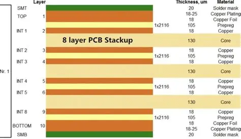
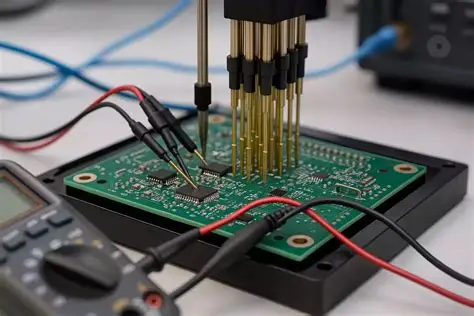
Design teams should evaluate candidate materials against a comprehensive checklist that includes electrical specifications, thermal profiles, and documented fabrication experience with similar constructions. Stack-up symmetry and balanced copper distribution help mitigate warpage regardless of the base material. Specifying tighter tolerances on dielectric thickness and copper weight allows fabricators to maintain impedance targets more reliably. Early material qualification testing, aligned with established industry procedures, identifies potential issues before volume production. Documentation of material handling requirements, such as moisture sensitivity levels and storage conditions, prevents downstream defects during assembly. When multiple materials satisfy electrical needs, preference is given to those with proven process windows that align with existing equipment capabilities.
Conclusion
Material selection exerts a decisive influence on the manufacturability of high-frequency PCBs by shaping process yields, reliability, and overall project cost. Systematic evaluation of dielectric, thermal, and mechanical properties against fabrication constraints enables designs that meet performance targets while remaining practical to produce. Adherence to recognized qualification standards supports consistent outcomes across suppliers and production lots. Engineers who integrate DFM considerations from the initial material review stage reduce the likelihood of late-stage modifications and improve time-to-market performance.
FAQs
Q1: How does dielectric constant variation affect DFM in high-frequency PCB materials?
A1: Dielectric constant stability directly influences impedance control during fabrication. Materials with tighter tolerances on this property allow fabricators to meet trace width and spacing specifications more consistently, reducing the need for iterative adjustments and improving overall yield.
Q2: What role does coefficient of thermal expansion play when choosing PCB materials for DFM?
A2: Coefficient of thermal expansion mismatch between substrate and copper or components generates stress during thermal cycling. Selecting materials with compatible expansion characteristics minimizes risks of via cracking or delamination, supporting higher assembly yields and long-term reliability.
Q3: Why is moisture absorption an important consideration for high frequency PCB materials DFM?
A3: High moisture absorption can lead to delamination or blistering during soldering processes. Materials with lower absorption rates reduce the requirement for extended baking cycles and lower the incidence of moisture-related defects in production.
Q4: How do Rogers material DFM guidelines help optimize high-frequency designs?
A4: Following established material-specific handling and process recommendations ensures compatibility with etching, drilling, and lamination steps. This alignment improves first-pass success rates and maintains electrical performance targets throughout manufacturing.
References
IPC-6012E — Qualification and Performance Specification for Rigid Printed Boards. IPC, 2017
IPC-4101D-WAM1 — Specification for Base Materials for Rigid and Multilayer Printed Boards. IPC, 2017
JEDEC J-STD-020E — Moisture/Reflow Sensitivity Classification for Nonhermetic Surface Mount Devices. JEDEC, 2014





