 ALLPCB


Introduction
Mixed-signal printed circuit boards integrate analog and digital circuitry, creating challenges in noise management and signal integrity. A ground plane split divides the ground plane into separate regions, typically for analog ground vs digital ground isolation. This technique aims to prevent high-frequency digital noise from corrupting sensitive analog signals. Engineers must weigh the benefits of ground plane isolation against potential risks like increased inductance and electromagnetic interference. Understanding the principles behind ground plane splits ensures better performance in complex designs. Proper implementation follows established engineering practices to maintain low impedance paths.
What Is a Ground Plane Split and Why It Matters
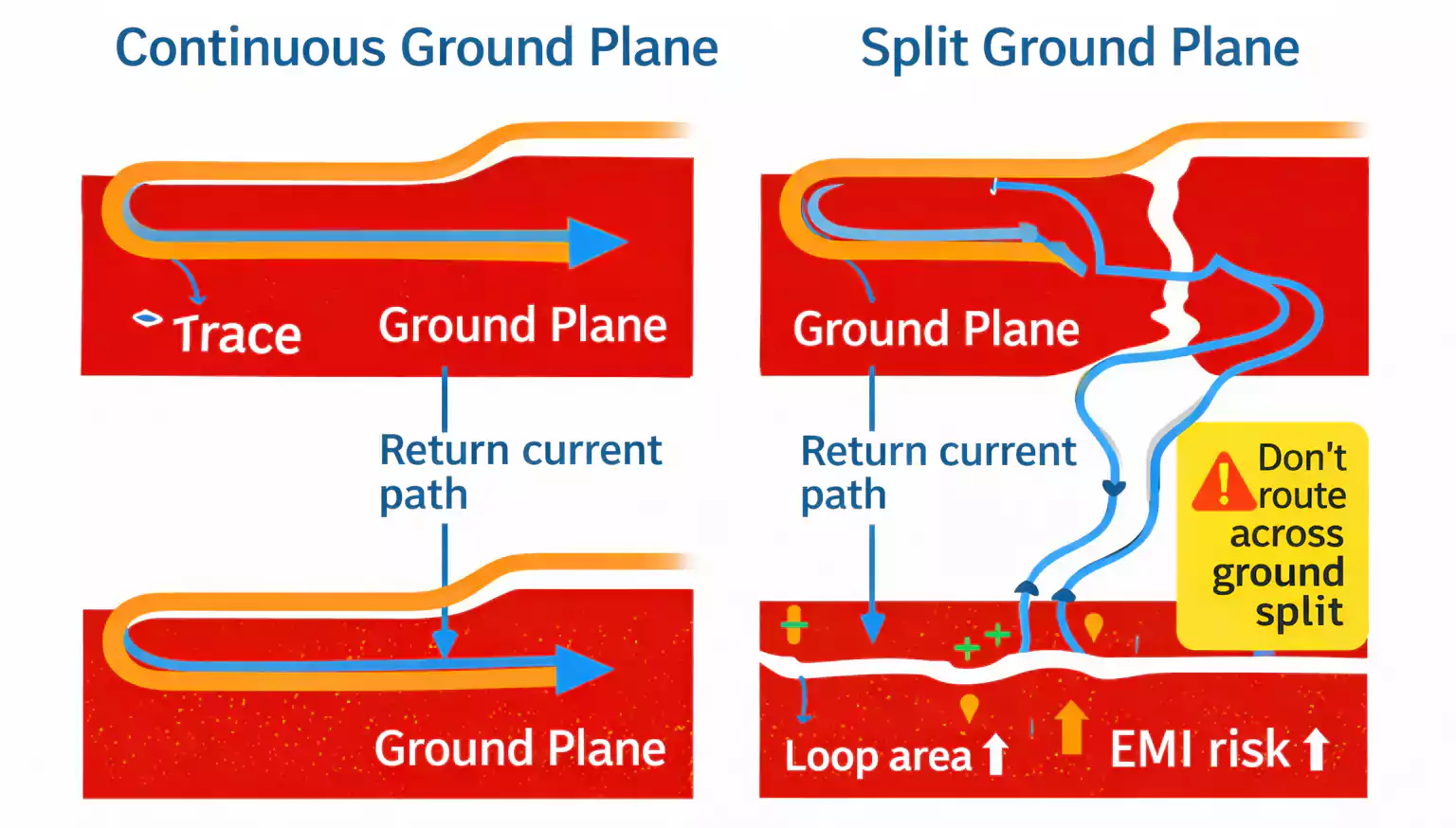
A ground plane split physically divides a continuous copper pour on a PCB layer into distinct sections, often separating analog and digital grounds. In mixed-signal PCBs, digital switching generates return currents with sharp edges that can couple into analog paths through shared ground. Without isolation, this noise degrades precision in amplifiers, ADCs, and sensors. Ground plane isolation minimizes common-impedance coupling by confining currents to their respective domains. However, splits introduce discontinuities that disrupt low-impedance return paths if not managed carefully. The decision to implement a ground plane split directly impacts overall system reliability and compliance with performance standards.
Engineers prioritize ground plane splits in designs where analog signals demand high dynamic range, such as audio or instrumentation systems. Digital noise floors can rise by tens of dB without proper separation, affecting measurement accuracy. Conversely, solid planes offer better shielding but require spatial partitioning. Balancing these factors aligns with IPC-2221 guidelines for conductor spacing and plane integrity. Effective ground management reduces EMI susceptibility and emissions during certification testing.
Technical Principles of Ground Plane Division
Return currents follow the path of least impedance, seeking proximity to signal traces under the skin effect at high frequencies. In a solid ground plane, these currents spread evenly, maintaining low inductance. A ground plane split forces digital return currents to detour around the gap, creating voltage drops that appear as noise on analog sections. The gap width must exceed three times the dielectric height to prevent fringing fields from bridging the divide. Stitching vias along split edges provide high-frequency coupling while preserving DC isolation.
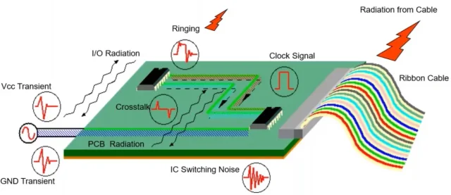
Slotting effects occur when signals cross splits, turning the gap into a slot antenna that radiates EMI. Analog ground vs digital ground differences amplify when power supplies share return paths, leading to ground bounce. Multi-layer boards mitigate this by dedicating inner layers to partitioned grounds adjacent to signals. Current density peaks near IC pins, so plane thickness and material conductivity influence voltage gradients. These principles guide when ground plane splits enhance rather than degrade performance.
When to Implement a Ground Plane Split
Reserve ground plane splits for high-precision mixed-signal PCBs where analog noise budgets are tight, such as 24-bit data acquisition systems. Low-layer-count boards, typically two or four layers, perform better with a single unbroken plane to avoid return path elongation. Split only if analog sections occupy less than 20 percent of the board and no fast digital signals cross the boundary. Multi-layer stacks with dedicated ground layers allow safer partitioning under sensitive traces.
Assess frequency content: splits suit designs below 100 MHz where skin depth exceeds plane thickness. High-speed digital above 500 MHz demands solid planes for controlled impedance. Evaluate layer stackup; inner splits reduce radiation compared to outer layers. Pre-layout simulations confirm if isolation justifies the split. Following J-STD-001 assembly standards ensures vias and connections maintain integrity post-fabrication.
Avoid splits in power-heavy designs, as uneven current distribution causes thermal hotspots. Board size influences decisions: compact layouts favor single planes for shorter loops. Prototype testing validates choices by measuring noise spectra across operating conditions.
Best Practices for Dividing and Connecting Ground Planes
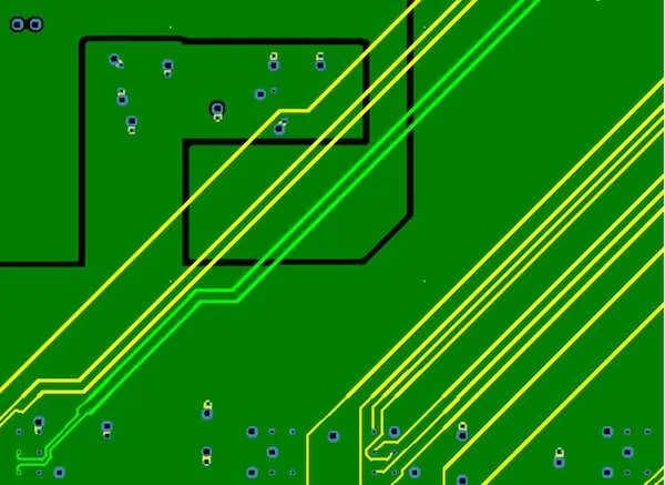
Start with physical partitioning: place digital ICs and clocks distant from analog inputs, minimizing shared perimeter. If splitting, maintain a minimum gap of 0.5 mm, scaled by frequency per IPC-2221 conductor rules. Route no traces over splits; use orthogonal layers if crossing is unavoidable. Connect split regions at a single low-impedance point near the power entry module, using a 0-ohm resistor or ferrite bead for filtering.
Deploy stitching vias every lambda/20 along the split edge, where lambda is the wavelength of the highest frequency. These vias, paired with 0.1 uF capacitors, bridge high-frequency returns without DC shorting. Pour ground under mixed-signal ICs to unify local references. Guard rings around analog components shunt noise to ground. Verify continuity with impedance scans during design review.
For connecting ground planes in non-split designs, flood pours and tie with multiple vias under components. Prioritize ground plane adjacency to signal layers for return path coupling. Decouple supplies locally to starve noise propagation.
Common Pitfalls in Ground Plane Isolation
Signals routed parallel to splits induce coupling through magnetic fields, elevating crosstalk by 20 dB or more. Narrow gaps allow capacitive bridging, nullifying isolation. Over-stitched edges create unintended antennas if via spacing exceeds quarter-wavelength. Unconnected splits foster floating islands prone to charge buildup.
Troubleshooting starts with scope probes on ground nodes to map voltage differentials. EMI scans reveal slot resonances; widen gaps or add shielding. Re-spin prototypes with single planes if splits cause failures. Layer swaps resolve inner-plane issues without respin costs.
Case in point: a four-layer ADC board with split grounds exhibited 10 mV ripple until stitching vias and single-point tie fixed return paths. Simulations predicted the fix, cutting debug time.
Conclusion
Ground plane splits offer targeted isolation in mixed-signal PCBs but demand rigorous application to avoid inductance traps and EMI. Prefer single solid planes with spatial separation for most designs, resorting to splits only in precision analog scenarios. Adhere to gap rules, stitching, and connection strategies for success. These practices ensure signal integrity and robust performance. Engineers gain confidence through simulation and validation, aligning with industry benchmarks.
FAQs
Q1: When should I use a ground plane split in a mixed-signal PCB?
A1: Opt for a ground plane split only in high-precision analog designs where digital noise exceeds the noise budget, such as precision ADCs. Ensure no signals cross the split and use multi-layer boards for inner partitioning. Single planes suffice for most cases, providing lower inductance. Follow spatial separation and decoupling to achieve analog ground vs digital ground isolation without division.
Q2: What are the risks of improper ground plane isolation?
A2: Poor ground plane isolation leads to return current detours, ground bounce, and EMI radiation from slot effects. Signals near splits suffer crosstalk, degrading SNR in analog sections. Stitching failures amplify high-frequency issues. Testing reveals voltage gradients; correct with wider gaps and vias spaced at lambda/20.
Q3: How do you connect split ground planes effectively?
A3: Connect split ground planes at one point near power input using a ferrite bead or 0-ohm jumper for DC continuity and AC filtering. Add stitching vias with capacitors along edges for HF coupling. This maintains low-impedance paths while preserving isolation. Verify with PI simulations.
Q4: Is a single ground plane always better than a split for mixed-signal PCBs?
A4: A single ground plane excels in low-layer boards by minimizing discontinuities and EMI. Partition sections physically and route carefully for effective analog ground vs digital ground separation. Splits risk more harm unless analog sensitivity justifies them. Multi-layer designs offer flexibility.
References
IPC-2221B — Generic Standard on Printed Board Design. IPC, 2003
J-STD-001G — Requirements for Soldered Electrical and Electronic Assemblies. IPC, 2011
IPC-A-600K — Acceptability of Printed Boards. IPC, 2020


