 ALLPCB


Introduction
The smart lighting revolution is reshaping illumination systems across residential, commercial, and industrial environments by embedding intelligence directly into hardware. Microcontroller controlled LED PCB design stands at the forefront, enabling precise modulation of light output, color temperatures, and dynamic patterns through compact, integrated circuits. Electric engineers leverage these designs to create addressable LED PCB circuits that respond individually to control signals, fostering energy-efficient solutions. IoT enabled LED lighting systems extend this capability, allowing remote management and data-driven adjustments via wireless protocols. PWM dimming control on LED PCBs ensures flicker-free operation and extends component lifespan by regulating current flow effectively. Designing LED PCBs with sensors integrates environmental feedback, automating responses to ambient conditions for optimal performance.
Understanding Microcontroller Controlled LED PCB Design
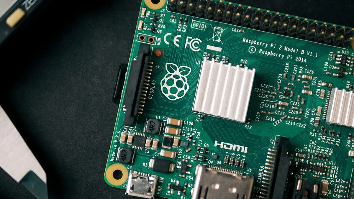
Microcontroller controlled LED PCB design involves selecting compact processors with sufficient I/O pins, memory, and processing power to handle lighting algorithms. Engineers choose microcontrollers based on pin count for LED driving, ADC channels for sensor inputs, and PWM peripherals for dimming. The PCB layout must accommodate the microcontroller's package, such as QFN or SOIC, while providing robust power rails and decoupling capacitors to minimize noise. Signal integrity becomes critical, as digital lines to LEDs require controlled impedance to prevent data corruption in addressable chains. Thermal vias under the microcontroller dissipate heat generated during intensive computations. Power supply design ensures stable voltage delivery, often using linear regulators or DC-DC converters tailored to LED forward voltages.
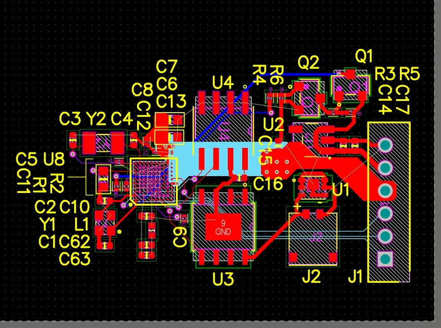
This design paradigm shifts from discrete drivers to unified boards, reducing component count and assembly complexity. Engineers follow structured workflows, starting with schematic capture that defines MCU-LED interfacing via GPIO or dedicated peripherals. Firmware development complements hardware, implementing protocols for sequential LED control. Board stackups typically feature two to four layers, with ground planes shielding sensitive signals. Component placement prioritizes short traces between MCU outputs and LEDs to reduce EMI. Validation through simulation verifies timing and power budgets before prototyping.
Implementing Addressable LED PCB Circuits
Addressable LED PCB circuits utilize daisy-chained LEDs where each pixel processes and forwards data serially, enabling individual control without wiring proliferation. Protocols rely on precise timing, with the microcontroller generating bit streams that configure color and brightness per LED. PCB traces for data lines demand consistent width and length matching to maintain signal edges across the chain. Engineers mitigate reflections by adding series resistors at the data input and ensuring ground return paths. Power distribution requires wide polygons or multiple vias to handle cumulative current draw from all LEDs. Bypass capacitors near each segment stabilize supply voltage fluctuations.
Routing strategies separate high-current LED power from low-level control signals, preventing ground bounce. Multi-layer boards dedicate inner layers to power and ground, enhancing decoupling. Addressable setups scale efficiently for strips or matrices, ideal for displays or ambiance lighting. Testing involves oscilloscope checks for signal integrity and current probes for load verification. Firmware handles refresh rates above human perception to avoid visible artifacts. These circuits form the backbone of dynamic lighting, supporting effects like fades and chases.
Building IoT Enabled LED Lighting Systems
IoT enabled LED lighting systems integrate wireless modules alongside microcontrollers, facilitating cloud connectivity and app-based control. Engineers pair MCUs with modules supporting Wi-Fi, Bluetooth, or Zigbee, using UART or SPI for communication. Antenna placement on the PCB edge ensures optimal RF performance, away from noisy digital lines. Firmware stacks manage protocol stacks, security handshakes, and over-the-air updates. Power management circuits include low-dropout regulators and sleep modes to extend battery life in portable setups. Sensor fusion via I2C bus aggregates data for predictive lighting adjustments.
Network topologies consider mesh configurations for large installations, distributing control across nodes. PCB design incorporates shielding cans over RF sections to comply with emission limits. Bootloaders enable field reprogramming, enhancing longevity. Integration with gateways allows voice assistant compatibility without direct MCU overload. Data logging tracks usage patterns, informing efficiency optimizations. These systems elevate lighting from static to adaptive ecosystems.
Mastering PWM Dimming Control on LED PCBs
PWM dimming control on LED PCBs modulates duty cycle to achieve variable brightness, maintaining color consistency across intensities. Microcontroller timers generate high-frequency PWM signals, typically 1 kHz or higher, fed to LED drivers or directly to low-power LEDs. PCB layout positions MOSFETs or drivers close to LEDs, minimizing inductive ringing with snubbers if needed. Current sense resistors provide feedback for constant current operation, stabilizing output against supply variations. Thermal runaway prevention involves heatsinks or exposed pads connected to vias. Engineers calculate PWM resolution based on desired steps, balancing smoothness with timer constraints.
Analog dimming complements PWM for ultra-low levels, blending methods in hybrid schemes. Trace widths scale with switched currents, following current density guidelines to avoid electromigration. Decoupling at PWM outputs filters harmonics, reducing audible noise in inductive loads. Scope analysis confirms duty cycle accuracy and rise times. Closed-loop control incorporates optocouplers for isolation in high-voltage setups. This technique underpins reliable, efficient dimming in smart applications.
Following IPC-2221 guidelines ensures trace spacing and width adequacy for PWM signals, preventing shorts under thermal expansion.
Best Practices for Designing LED PCBs with Sensors
Designing LED PCBs with sensors embeds ambient light, proximity, or temperature detectors for autonomous operation. Placement positions sensors away from LED light spill, using cutouts or shields for accuracy. I2C or analog interfaces connect to the microcontroller, sharing buses with minimal crosstalk via pull-ups. Mixed-signal layout segregates analog grounds from digital, starring them at the power entry point. Calibration routines in firmware compensate for aging or environmental drifts. Multi-sensor arrays enable zoned control, mapping light distribution precisely.
Power budgeting accounts for sensor quiescent currents alongside LED peaks, using efficient LDOs. ESD protection diodes safeguard inputs per industry norms. Optical sensors pair with lenses for field-of-view tuning. Vibration isolation suits motion detectors in dynamic fixtures. Prototyping validates sensitivity thresholds under real loads. These integrations yield context-aware lighting.
Adhering to IPC-6012 performance specifications during qualification verifies sensor-LED interactions under stress.
Advanced Integration and Troubleshooting
Combining PWM dimming control on LED PCBs with IoT enabled LED lighting systems demands synchronized firmware tasks. Engineers prioritize interrupts for sensor events over PWM servicing to avoid jitter. Common issues like LED desynchronization stem from clock drift, resolved by synchronization pulses. Overheating triggers thermal throttling via onboard diodes feeding ADC. Firmware diagnostics log errors via UART for remote debugging. Modular designs facilitate upgrades, swapping MCUs without full redesigns.
Assembly per J-STD-001 requirements ensures reliable solder joints for fine-pitch sensors and MCUs. X-ray inspection detects voids under BGAs. Functional testing sequences ramp currents gradually. Field failures often trace to marginal power margins, addressed by derating. Iterative DFMEA identifies risks early. These practices solidify robust deployments.

Conclusion
Integrating microcontrollers on LED PCBs propels the smart lighting revolution, delivering addressable control, IoT connectivity, precise PWM dimming, and sensor-driven intelligence. Microcontroller controlled LED PCB design empowers electric engineers to craft efficient, scalable systems. Addressable LED PCB circuits enable intricate effects, while designing LED PCBs with sensors automates responsiveness. These advancements optimize energy use and user interaction. Future iterations will refine power efficiency and AI integration. Engineers equipped with these principles drive innovation reliably.
FAQs
Q1: What are the key advantages of microcontroller controlled LED PCB design for electric engineers?
A1: Microcontroller controlled LED PCB design offers compact integration, reducing wiring and costs while enabling custom algorithms for lighting effects. It supports scalable addressable configurations and real-time sensor processing. Power efficiency improves through optimized PWM and sleep modes. Troubleshooting simplifies via onboard diagnostics. Overall, it accelerates prototyping and deployment in IoT applications.
Q2: How does PWM dimming control on LED PCBs improve smart lighting performance?
A2: PWM dimming control on LED PCBs provides smooth, flicker-free brightness adjustment by varying duty cycles at high frequencies. It preserves color accuracy and extends LED life by limiting average power. Integration with microcontrollers allows dynamic response to inputs. Engineers achieve high resolution without complex analog circuits. Thermal management pairs effectively for sustained operation.
Q3: What considerations apply when building IoT enabled LED lighting systems on PCBs?
A3: IoT enabled LED lighting systems require RF-optimized layouts, secure firmware, and low-power schemes for wireless modules. Sensor integration enhances automation via shared buses. Power planes support peak loads from LEDs and radios. EMI shielding protects signals. Compliance with design standards ensures reliability in connected environments.
Q4: Why integrate sensors in designing LED PCBs with addressable circuits?
A4: Designing LED PCBs with sensors enables ambient-adaptive lighting, such as auto-dimming based on light levels or motion activation. Addressable LED PCB circuits allow zoned responses per sensor data. Microcontrollers process inputs for precise control. This boosts efficiency and user comfort. Noise isolation maintains accuracy.
References
IPC-2221B - Generic Standard on Printed Board Design. IPC, 2003
IPC-6012E - Qualification and Performance Specification for Rigid Printed Boards. IPC, 2017
J-STD-001GA - Requirements for Soldered Electrical and Electronic Assemblies. IPC, 2011


