 ALLPCB


Introduction
Single-layer printed circuit boards remain a cornerstone in electronics design for applications demanding simplicity and economy. These boards feature conductive traces on only one side of the insulating substrate, eliminating the need for vias and inner layers that drive up costs in multi-layer designs. For electrical engineers facing tight budgets, understanding single layer PCB cost factors is essential to maintain reliable performance without unnecessary expenses. Affordable PCB manufacturing becomes achievable through optimized design and process choices that prioritize essential functionality. This article delves into practical strategies for reducing PCB expenses while adhering to performance requirements. By focusing on low-cost PCB materials and efficient production methods, engineers can deliver robust single-sided PCB solutions at competitive prices.
Understanding Single-Layer PCBs and Their Cost Advantages
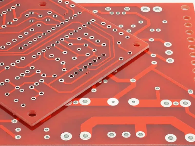
A single-layer PCB, also known as a single-sided PCB, consists of a base substrate coated with a thin copper layer on one surface, etched to form the circuit pattern. Components mount directly on the traced side, with no electrical connections passing through the board. This simplicity translates directly to lower single sided PCB price, as manufacturing involves fewer steps than double-sided or multi-layer boards. Engineers value these boards for low-volume prototypes, consumer electronics, sensors, and LED displays where high-speed signals or dense routing are not critical. The absence of plating through holes reduces material usage and processing time, making them ideal for affordable PCB manufacturing. Despite their basic structure, single-layer boards must still meet reliability standards to ensure long-term functionality in real-world conditions.
Cost savings stem from reduced material consumption and streamlined fabrication. For instance, standard substrate thicknesses suffice without the reinforcement needed for multi-layer stacks. Labor and equipment time drop significantly, as etching and soldering occur on a single plane. Engineers can further lower single layer PCB cost by specifying minimal copper weights, such as 1 oz/ft2, which balances conductivity with economy. These attributes make single-layer designs a strategic choice for projects where budget constraints dominate over feature complexity. Ultimately, their relevance persists in industries prioritizing affordability over advanced interconnect density.
Key Design Principles for Minimizing Single Layer PCB Cost
Effective design begins with layout optimization to maximize board real estate and minimize waste. Engineers should route traces with generous widths to avoid narrow features that demand finer etching precision and higher costs. Adhering to standard trace spacing, typically 0.010 inches or more, prevents the need for advanced imaging equipment during production. Component placement plays a crucial role; grouping parts closely reduces overall board size, which directly impacts single sided PCB price through smaller panel yields. Avoiding right-angle bends in traces enhances manufacturability and reduces etching variability. By simulating thermal and electrical performance early, designers eliminate iterations that inflate expenses.
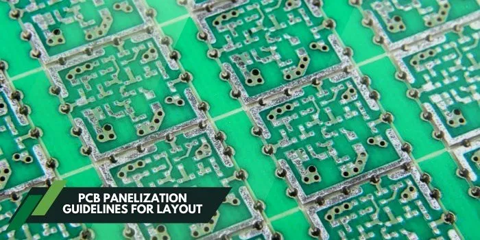
Panelization emerges as a powerful technique for affordable PCB manufacturing. Multiple identical boards fit onto a single production panel, spreading setup costs across units and boosting throughput. Engineers must account for v-scoring or tab routing in designs to facilitate clean depanelization without damaging traces. Standard panel sizes, often 18x24 inches, allow efficient nesting that minimizes scrap. Incorporating fiducials for alignment ensures precise registration during etching and inspection. These practices collectively drive down per-unit single layer PCB cost while preserving design integrity.
Material selection influences costs profoundly, with low-cost PCB materials like standard FR-4 offering a reliable baseline. Thinner laminates, such as 0.031 inches, reduce substrate volume without compromising rigidity for most applications. Copper foil thickness should match current requirements; 0.5 oz options suffice for low-power circuits, cutting material expenses. Surface finishes like HASL provide cost-effective solderability, though ENIG serves higher-reliability needs at a premium. Engineers evaluate glass transition temperature (Tg) values around 130°C for general use, ensuring stability under operating conditions. Balancing these choices prevents over-specification that erodes budget advantages.
Manufacturing Processes That Optimize Affordability
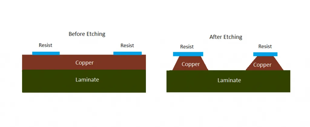
Photochemical etching defines the core process for single-layer boards, involving photoresist application, exposure, development, and copper removal. This subtractive method excels in high-volume runs due to its scalability and low setup for simple patterns. Dry film resist ensures uniform imaging on large panels, supporting affordable PCB manufacturing for prototypes and production alike. Post-etch cleaning removes residues, preparing the board for solder mask if specified. Engineers benefit from specifying tin plating over bare copper to prevent oxidation, a low-cost step that extends shelf life. Process controls maintain etch factor consistency, avoiding undercuts that necessitate rework.
Drilling requirements minimize in single-layer designs, often limited to mounting holes. Standard carbide tools handle these efficiently, with no electroplating needed. Solder mask application via screen printing adds insulation at minimal cost, protecting traces from shorts. Silk screen legends provide assembly aids without complexity. Baking cures the mask, enhancing adhesion per industry guidelines. These sequential steps keep single layer PCB cost low by leveraging mature, equipment-shared processes.
Quality assurance integrates seamlessly to uphold standards without excessive expense. Visual inspection per IPC-A-600K criteria detects defects like mouse bites or pinholes early. Automated optical systems scale for volume while maintaining objectivity. Electrical testing verifies continuity on critical nets, a quick probe-based method. Dimensional checks ensure hole tolerances and outline accuracy. By embedding these at key stages, manufacturers reduce scrap and yield cost-effective single-sided PCB production.
Best Practices for Reducing PCB Expenses in Single-Layer Projects
Start with thorough specification review to eliminate non-essential features. Engineers often request thinner solder mask or legend only where functional, trimming material use. Tolerances should default to standard values, such as ±0.005 inches for holes, avoiding tight specs that slow fabrication. Batch sizing optimizes economies; combining orders amortizes tooling. Feedback loops with fabricators refine designs iteratively for manufacturability. These habits systematically lower reducing PCB expenses across projects.
Tooling optimization further curbs costs. Reusable steel stencils for solder paste application serve multiple panels, unlike single-use films. Fixtureless fixturing relies on fiducials for vacuum holding during exposure. Edge rails in panelized arrays enable automated handling, cutting labor. Post-production, bulk packaging prevents damage during shipping. Engineers track yield metrics to identify recurring issues, refining future designs proactively.
Handling and storage protocols preserve board integrity affordably. ESD-safe bagging with desiccants complies with JEDEC J-STD-020E for moisture control. Vacuum sealing extends usability without nitrogen purging. Labeling includes lot codes for traceability, aiding failure analysis. These measures minimize rejects, sustaining low-cost PCB materials' value.
Quality Control Strategies in Cost-Effective Production
Adherence to IPC-6012E ensures qualification for rigid boards, including single-layer types, through defined performance tests. This standard outlines electrical, mechanical, and environmental criteria without mandating premium processes. Solderability checks per IPC-6012E verify wetting after simulated aging, critical for assembly yield. Bow and twist measurements limit warpage to acceptable levels for component mounting. Thermal cycling simulates operational stress, confirming delamination resistance. Implementing these verifies reliability at controlled costs.
Microsection analysis samples production lots, revealing copper plating uniformity and laminate integrity. Etch depth profiling prevents over-etching that compromises trace strength. Ionic contamination testing per IPC-6012E guards against reliability risks in humid environments. Statistical process control monitors variables like panel yield, enabling predictive adjustments. These targeted controls balance single layer PCB cost with assured performance.
Real-World Applications and Insights
In power supply modules, single-layer boards handle rectification circuits efficiently. Thick traces carry high currents, with heat sinks attached directly. Cost savings enable scaling for consumer adapters. Automotive sensors leverage their robustness, enduring vibration per IEC standards. Compact designs fit harsh enclosures, prioritizing affordability. These examples illustrate versatile deployment without multi-layer premiums.
Engineers troubleshoot cost overruns by auditing design files for density. Overly fine features inflate imaging expenses; simplifying resolves this. Panel utilization audits reveal nesting inefficiencies. Material variance tracking stabilizes pricing. Collaborative reviews with procurement teams align expectations, optimizing single sided PCB price.
Conclusion
Cost-effective single-layer PCB solutions empower engineers to deliver functional designs within budget limits. Strategic material choices, layout efficiency, and process streamlining minimize single layer PCB cost while upholding performance. Affordable PCB manufacturing thrives on panelization, standard tolerances, and targeted quality checks aligned with IPC standards. Low-cost PCB materials like FR-4 provide a solid foundation for reliability. Reducing PCB expenses demands holistic consideration from design to delivery. By applying these principles, projects achieve optimal balance, fostering innovation in resource-constrained environments.
FAQs
Q1: What are the main factors influencing single layer PCB cost?
A1: Single layer PCB cost depends on board size, copper thickness, panel quantity, and tolerances. Larger panels with multiple boards per run lower per-unit prices through economies of scale. Material choices like standard FR-4 and minimal surface finishes further reduce expenses. Engineers control costs by avoiding tight specs and optimizing layouts for etching efficiency. Production volume significantly impacts setup amortization.
Q2: How can engineers select low-cost PCB materials for single-sided designs?
A2: Low-cost PCB materials center on FR-4 with 130°C Tg for most applications, paired with 1 oz copper. Thinner laminates cut substrate volume while maintaining rigidity. HASL finish offers economical solderability over pricier alternatives. Verify material datasheets against IPC-6012E for qualification. Balance conductivity needs with budget to prevent over-specification.
Q3: What manufacturing techniques best support affordable PCB manufacturing?
A3: Photochemical etching and screen-printed solder mask enable affordable PCB manufacturing for single-layer boards. Panelization maximizes throughput, spreading tooling costs. Standard drilling for mounting holes avoids complex operations. Inline quality checks per IPC-A-600K minimize rework. Engineers specify these for consistent, low single sided PCB price.
Q4: How to reduce PCB expenses without sacrificing single-layer performance?
A4: Reducing PCB expenses involves generous trace widths, standard thicknesses, and batch ordering. Eliminate unnecessary vias or masks to trim materials. Use fiducials for precise, fixtureless processing. Simulate designs early to catch inefficiencies. Adhere to JEDEC handling for yield preservation. These steps maintain reliability at lower costs.


