 ALLPCB


Introduction
In modern electronics, 6-layer PCBs serve as a critical platform for high-speed designs, offering dedicated layers for signals, power, and ground planes. These boards balance complexity with performance, enabling compact layouts for applications like telecommunications and computing systems. Vias, the conductive pathways connecting layers, play a pivotal role in this architecture, yet they introduce challenges to signal and power integrity. Poor via design can lead to impedance mismatches, inductive effects, and crosstalk, degrading overall board performance. Engineers must understand 6-layer PCB via types, placement rules, impedance, inductance, and optimization strategies to mitigate these issues. This article explores these elements logically, providing structured guidance grounded in engineering principles.
Understanding 6-Layer PCB Via Types
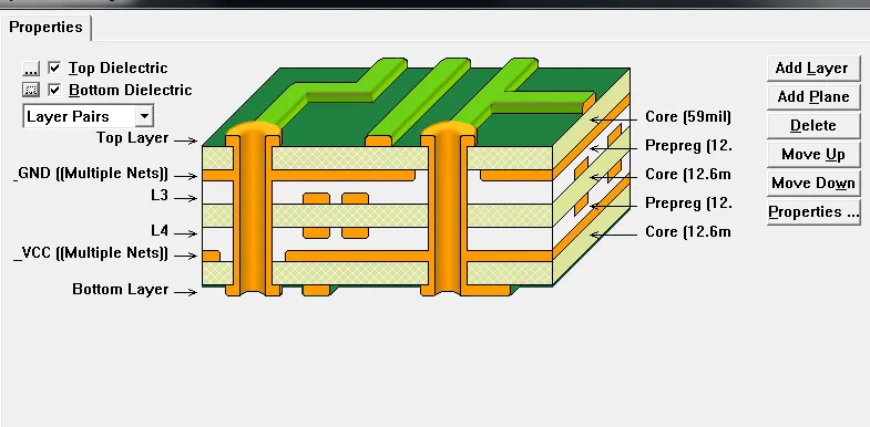
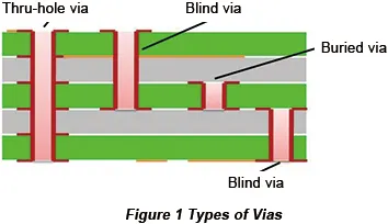
Vias in 6-layer PCBs interconnect the six copper layers, typically arranged as signal-ground-signal-power-signal-ground to optimize reference planes. Common 6-layer PCB via types include through-hole vias, which span all layers, blind vias connecting outer to inner layers, and buried vias linking only inner layers. Through-hole vias offer simplicity but create long stubs that reflect signals in high-speed paths. Blind vias, such as those from layer 1 to 3 or 4 to 6, reduce stub length and board real estate usage. Buried vias between layers 2-3 or 3-4 further minimize discontinuities by avoiding outer layers entirely.
Selecting the appropriate 6-layer PCB via types depends on routing density and frequency requirements. For instance, high-speed signals benefit from blind or buried vias to shorten transition paths. Microvias, though more common in HDI boards, can apply in dense 6-layer designs for fine-pitch connections. IPC-6012F outlines qualification criteria for these vias, ensuring plating integrity and reliability across classes. Engineers should evaluate via types early in stackup planning to align with performance goals.
Vias and Signal Integrity in 6-Layer PCBs
Signal integrity hinges on maintaining consistent transmission characteristics across vias. In 6-layer PCBs, vias disrupt characteristic impedance, causing reflections that distort waveforms. The 6-layer PCB via impedance arises from the via barrel's geometry and surrounding dielectric, often differing from trace impedance. Smaller diameters yield higher impedance, exacerbating mismatches at gigabit speeds. Engineers model this using field solvers to predict return loss.
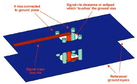
Via inductance compounds these issues, introducing series inductance proportional to via length and inversely to diameter. Longer through vias in 6-layer boards exhibit higher 6-layer PCB via inductance, leading to ringing and overshoot during fast edges. This effect intensifies with rising data rates, where even picohenry values matter. Crosstalk between adjacent vias also rises with density, as mutual inductance couples signals. Proper reference plane proximity in the stackup helps contain fields and lower inductance.
To quantify, via inductance scales with height, following approximations like L ≈ 5.08 × h × [ln(4h/d) + 1] in nH, with h as height and d as diameter in inches. While simulations refine this, the principle guides design: shorter, wider vias reduce inductance. IPC-2221B provides generic guidelines for via dimensions and spacing to support signal integrity.
Power Integrity Challenges Posed by Vias
Power distribution networks in 6-layer PCBs rely on low-impedance paths, where vias form critical links between planes. High via inductance elevates plane impedance, impeding transient currents for decoupling capacitors. In dense designs, multiple vias in parallel lower effective 6-layer PCB via inductance, distributing current evenly. Without this, voltage droop occurs under load, affecting core logic.
Via placement influences power integrity by defining current paths. Stitching vias tie ground planes, reducing slot inductance and EMI. Poor stitching spacing creates high-impedance loops, radiating noise. For power vias, backdrilling removes unused stubs, minimizing parasitic capacitance that shunts high frequencies. Filled vias enhance thermal and mechanical stability, vital for power-heavy sections.
Engineers optimize by simulating PDN impedance targets below milliohms at target frequencies. Layer sequencing in 6-layer stackups positions power vias near loads, shortening loops. These practices ensure stable rails, preventing jitter in clock domains.
6-Layer PCB Via Placement Rules
Strategic via placement upholds manufacturability and performance in 6-layer boards. 6-Layer PCB via placement rules dictate minimum spacing to prevent drill breakout and plating voids. IPC-4761 details via protection methods, influencing annular ring requirements around pads. Typically, via-to-via spacing exceeds twice the drill diameter, with anti-pads sized for clearance.
Density rules limit vias per square millimeter, balancing routing with drill capacity. High-speed vias require adjacent reference planes, avoiding splits within 10 times trace width. Power vias cluster near ICs, following current capacity guidelines from IPC-2221B. Aspect ratios under 10:1 ensure plating uniformity.
Placement grids align vias for symmetry, reducing warpage in multilayer presses. Engineers review DFM early, adjusting for fabricator capabilities. These rules prevent shorts, opens, and integrity losses.
Optimizing Vias for Enhanced Performance
6-Layer PCB via optimization integrates multiple techniques for superior signal and power integrity. Backdrilling shortens through vias, eliminating stubs longer than a wavelength fraction. Filled or plugged vias per IPC-4761 reduce capacitance and improve planarization for SMT. Multiple vias in arrays slash inductance by paralleling paths.
Impedance tuning uses larger diameters or tapered barrels, matched via simulations. Staggered blind vias in stackups minimize transitions. Via-in-pad designs save space in BGA areas, with tenting for protection.
Pre-layout planning models full via fields, iterating for minimal discontinuity. Post-layout verification confirms targets. These steps elevate 6-layer performance reliably.
Conclusion
Vias profoundly shape 6-layer PCB performance, demanding careful attention to types, placement, impedance, inductance, and optimization. By adhering to structured rules and standards, engineers achieve robust signal and power integrity. Proactive design yields reliable, high-speed boards ready for demanding applications.
FAQs
Q1: What are the main 6-layer PCB via types and their impact on performance?
A1: Through-hole, blind, and buried vias form the core 6-layer PCB via types. Through vias simplify fabrication but introduce long stubs harming signal integrity. Blind and buried types shorten paths, reducing reflections and inductance for high-speed signals. Selection depends on stackup and density, with standards like IPC-6012F guiding reliability.
Q2: How do 6-layer PCB via placement rules affect signal integrity?
A2: 6-Layer PCB via placement rules ensure adequate spacing and annular rings, preventing crosstalk and plating defects. Vias near reference planes minimize loop inductance, stabilizing impedance. Rules from IPC-2221B specify clearances, aiding DFM. Violations cause EMI and failures, so simulations validate layouts.
Q3: Why is 6-layer PCB via inductance critical for power integrity?
A3: 6-Layer PCB via inductance raises PDN impedance, causing voltage droop during transients. Paralleling vias and stitching lowers it, supporting decoupling. Optimization targets low pH values via wider drills and short heights. This maintains stable rails, essential for logic performance.
Q4: What strategies improve 6-layer PCB via optimization?
A4: Key 6-layer PCB via optimization includes backdrilling, filling, and arrays to cut stubs and inductance. Impedance matching via geometry tuning preserves signals. Simulations drive iterations, with IPC-4761 for protection. These enhance overall board reliability.
References
IPC-2221B — Generic Standard on Printed Board Design. IPC, 2012
IPC-6012F — Qualification and Performance Specification for Rigid Printed Boards. IPC, 2023
IPC-4761 — Via Protection, Control of Electrical and Mechanical Properties. IPC


