 ALLPCB


Why Reducing Hazardous Chemicals Matters in Flex PCB Production
Halogen-free flex PCBs and RoHS compliant flex PCB designs limit or eliminate bromine and chlorine compounds traditionally used as flame retardants in base materials. Non toxic pcb manufacturing extends this principle to etching and cleaning steps, where conventional chemistries can generate difficult-to-treat waste streams. The result is a more responsible supply chain that reduces potential exposure risks for workers and simplifies end-of-life handling of electronic assemblies.
Industry demand for these approaches stems from the need to meet material restrictions while preserving the mechanical flexibility and electrical reliability required in dynamic environments. Manufacturers achieve this by selecting base dielectrics that meet defined halogen thresholds and by refining process chemistry to lower overall hazardous content. Such practices also support consistent quality outcomes when evaluated against established performance criteria.
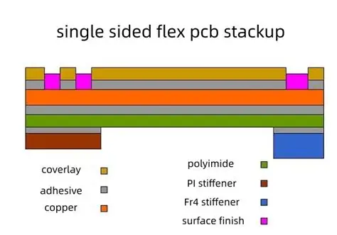
Technical Principles Behind Sustainable Flex PCB Processes
In conventional subtractive manufacturing, copper cladding is removed using etchants that must be neutralized and treated before disposal. These steps involve multiple chemical baths whose byproducts require specialized handling to prevent environmental release. Halogenated flame retardants in older laminate systems add another layer of concern, as they can form persistent compounds under certain thermal or disposal conditions.
Sustainable etching process alternatives focus on chemistry optimization, including closed-loop recovery systems that regenerate etchants and reduce fresh chemical consumption. Material suppliers now offer polyimide and other flexible dielectrics formulated without halogenated additives, maintaining dielectric strength and thermal stability through alternative formulations. Process controls ensure that any residual compounds remain within acceptable bounds during lamination, imaging, and final finishing.
These changes do not compromise the core electrical or mechanical properties when material selection and process parameters are aligned with qualification requirements. Engineers verify performance through standardized testing protocols that evaluate peel strength, flexibility endurance, and environmental resistance.
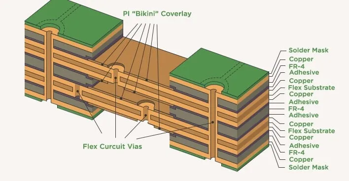
Practical Approaches to Chemical Reduction in Manufacturing
Facilities implement halogen free pcb strategies by qualifying base materials against recognized criteria early in the design phase. This includes specifying laminates and coverlays that satisfy low-halogen thresholds, followed by verification through incoming inspection and process monitoring. Etching lines are upgraded with filtration and regeneration equipment to minimize waste generation and chemical turnover.
Additional best practices involve reviewing the full process sequence for opportunities to substitute or eliminate solvents in cleaning and surface preparation. Additive patterning techniques, where applicable, further reduce the volume of etchant required compared with fully subtractive methods. Throughout production, documentation tracks material composition and process parameters to support traceability and repeated compliance verification.
Quality teams apply acceptance criteria from relevant standards to confirm that boards meet both functional and environmental expectations. Regular audits of chemical inventories and waste streams help maintain consistency across production runs.
Related Reading: Sustainable Flex PCBs: Designing for Longevity and Reduced E-Waste
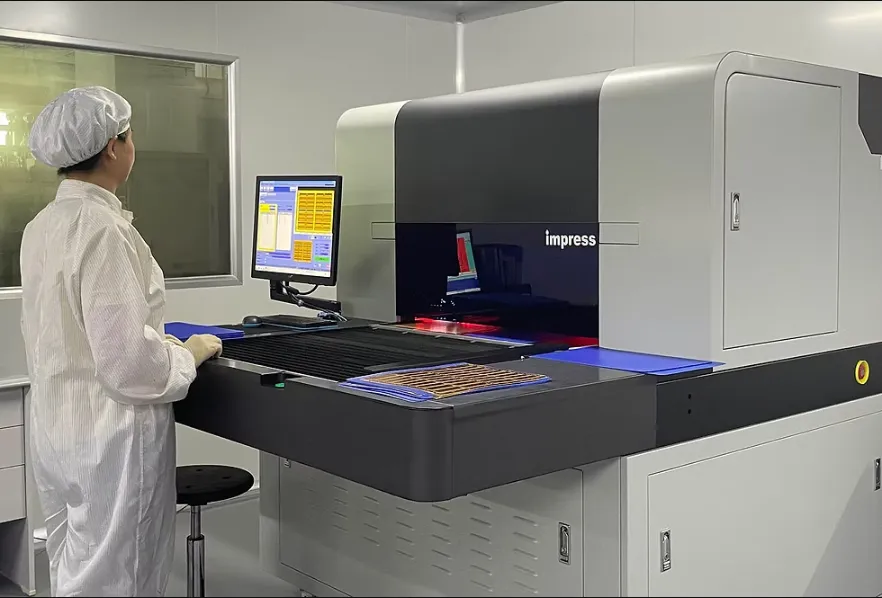
Implementation Considerations for Engineering Teams
Designers collaborate with manufacturing partners to select stack-ups that inherently support reduced chemical usage while meeting application-specific bend radius and current-carrying needs. Early involvement of process engineers allows identification of compatible materials and equipment configurations that align with facility capabilities. This proactive approach minimizes later adjustments that could increase chemical handling requirements.
Ongoing monitoring includes periodic review of etchant bath chemistry and laminate certifications to ensure continued alignment with reduction goals. When changes occur in material formulations or process equipment, re-qualification confirms that performance remains consistent with prior builds.
Related Reading: The Benefits of Lead Free Solder in Sustainable Flex PCB Assembly
Conclusion
Reducing hazardous chemicals in flex PCB manufacturing delivers measurable benefits in regulatory alignment, workplace safety, and environmental stewardship without sacrificing the performance characteristics essential to flexible circuit applications. By focusing on material selection, process optimization, and adherence to established qualification methods, manufacturers can achieve consistent results that support broader sustainability objectives in electronics production.
FAQs
Q1: What defines a halogen free pcb in flex circuit applications?
A1: A halogen free pcb uses base materials and adhesives with chlorine and bromine content limited according to industry-accepted thresholds. This approach supports safer handling during manufacturing and disposal while maintaining the flexibility and reliability expected in flex PCB designs.
Q2: How does a sustainable etching process differ from traditional methods?
A2: A sustainable etching process incorporates chemical recovery and regeneration steps that reduce the volume of fresh etchant required and limit waste generation. It pairs with halogen-free materials to lower overall hazardous substance use throughout flex PCB production.
Q3: Why pursue rohs compliant flex pcb construction?
A3: RoHS compliant flex pcb construction ensures that restricted substances, including certain halogens and heavy metals, remain below defined limits. This facilitates market access and simplifies compliance documentation for assemblies destined for regulated regions.
Q4: What role do standards play in non toxic pcb manufacturing verification?
A4: Standards provide consistent test methods and acceptance criteria that confirm material properties and process outcomes. They enable manufacturers to demonstrate that flex PCBs meet both performance and chemical-content expectations across production batches.
References
IPC-6013 — Qualification and Performance Specification for Flexible Printed Boards. IPC
IEC 61249-2-21 — Materials for printed boards and other interconnecting structures — Part 2-21: Reinforced base materials, clad and unclad — Non-halogenated epoxide woven E-glass reinforced laminated sheets of defined flammability (vertical burning test), copper-clad. IEC
IPC-4101 — Specification for Base Materials for Rigid and Multilayer Printed Boards. IPC





