ALLPCB


Forward Conduction Equivalent Circuit
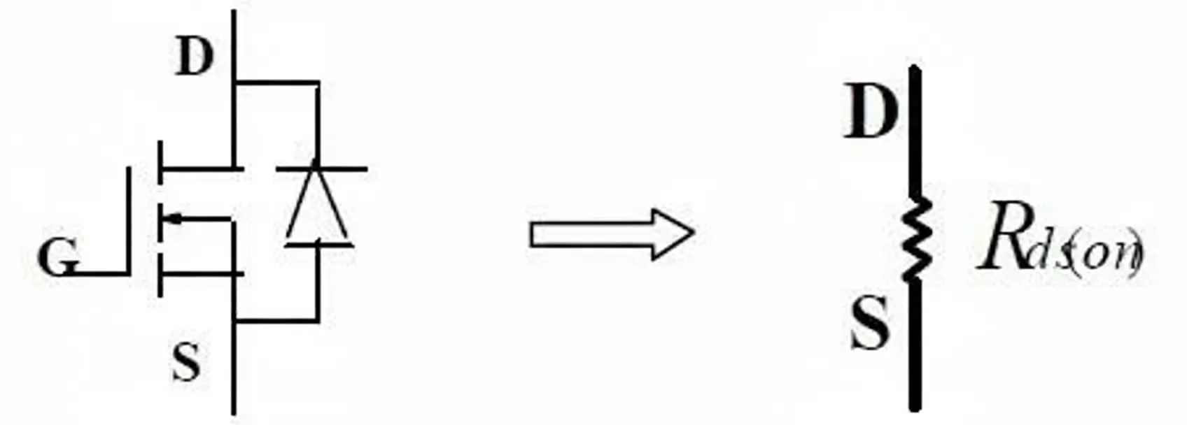
Equivalent circuit description: When a power MOSFET conducts in the forward direction, it can be modeled as a resistor. This resistance depends on temperature; as temperature rises the resistance increases. It also depends on gate drive voltage; higher gate voltage reduces the resistance. Detailed characteristic curves are available in the manufacturer's datasheet.
Reverse Conduction Equivalent Circuit (Gate Uncontrolled)
Equivalent circuit description: This represents the internal diode equivalent. It can be modeled as a voltage drop. This diode is the MOSFET body diode; in many cases its characteristics are poor and its use should be avoided when possible.
Reverse Conduction Equivalent Circuit (Gate Controlled)
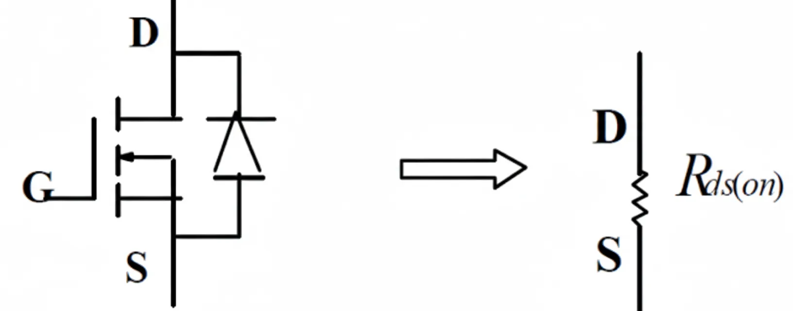
Equivalent circuit description: Under gate control, reverse conduction of a power MOSFET can also be modeled as a resistor. This resistance depends on temperature and on gate drive voltage; higher gate voltage reduces the resistance. Detailed curves are available from the manufacturer's datasheet. This operating mode is called synchronous rectification and is important in low-voltage, high-current switching power supplies.
Forward Cutoff Equivalent Circuit
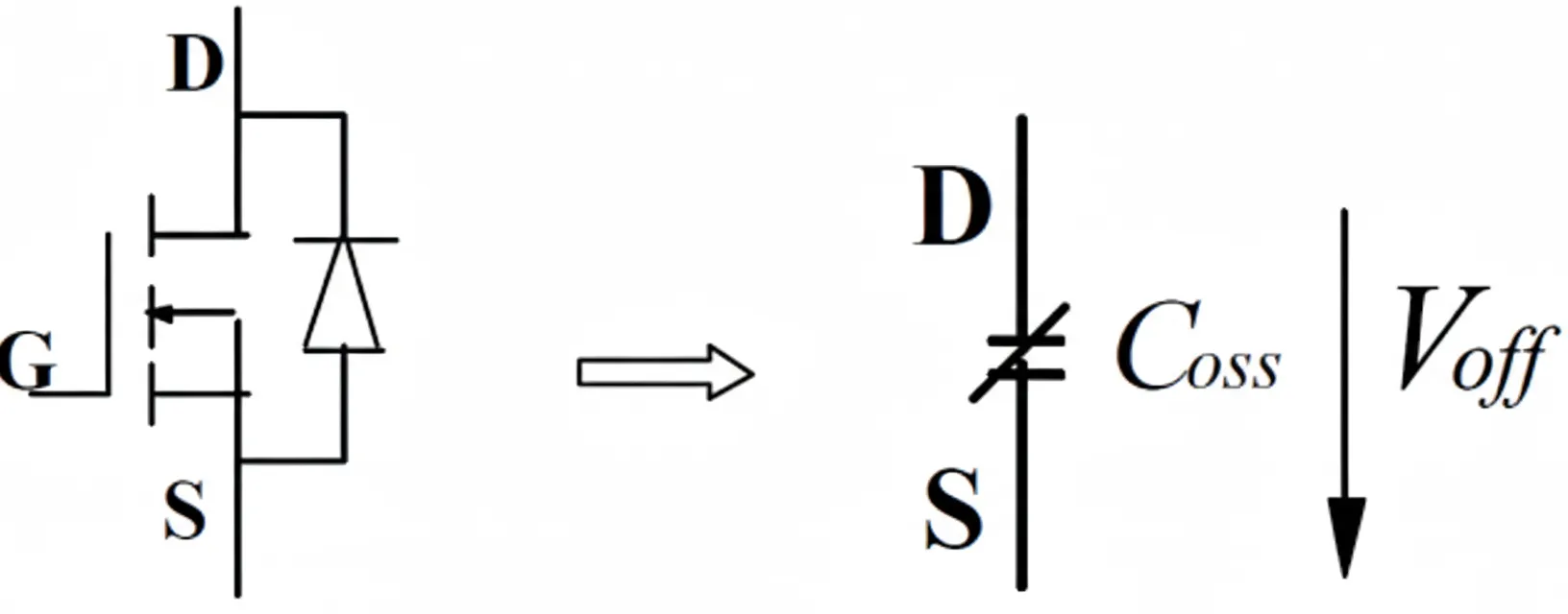
Equivalent circuit description: In forward cutoff, the power MOSFET can be modeled as a capacitor. Its capacitance depends on the applied forward voltage, ambient temperature, and other factors. Capacitance values are given in the manufacturer's datasheet.
Steady-State Characteristics Summary
1) Static I-V curve of a power MOSFET:
2) Steady-state operating point when the MOSFET is in forward saturation:
When the gate is uncontrolled, the reverse conduction steady-state point is the same as the diode.
Summary of steady-state characteristics:
- Gate-to-source voltage Vgs controls the device conduction. When Vgs > Vth, the device is on. The on-state resistance Rds(on) depends on Vgs; larger Vgs yields smaller Rds(on). Many devices specify Vgs in the 12V–15V range, with absolute limits around ±30V.
- Device drain current ratings are given as RMS or average values. As long as the actual drain current RMS does not exceed the rating and thermal management is adequate, the device operates safely.
- Rds(on) has a positive temperature coefficient, so paralleling devices is feasible in principle. In practice, dynamic current sharing and drive symmetry must be considered.
- Logic-level power MOSFETs can achieve low Rds(on) at Vgs = 5V.
- Synchronous rectification is increasingly common because of very low Rds(on) (as low as 2–4 mΩ). It is a critical component in low-voltage, high-current DC/DC converters.
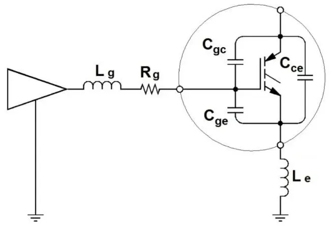
Equivalent Circuit Including Parasitic Parameters
Equivalent circuit description: A real power MOSFET can be represented by three junction capacitors, three channel resistances, an internal diode, and an ideal MOSFET. The junction capacitances depend on junction voltage. The gate channel resistance is typically small. The sum of the drain and source channel resistances equals the MOSFET on-state resistance when saturated.
Turn-On and Turn-Off Process
1) Switching test circuit:
2) MOSFET voltage and current waveforms:
3) Switching process explanation. Turn-on process [t0–t4]:
Before t0, the MOSFET is off. At t0 the MOSFET is driven on.
[t0–t1] The MOSFET gate-to-source voltage charges via the gate drive and Cgs rises. At t1 it reaches the threshold Vth and the MOSFET begins to conduct.
[t1–t2] Drain-source current increases. The Miller capacitance discharges due to DS capacitance behavior in this interval, with little effect on Cgs charging.
[t2–t3] By t2 the MOSFET DS voltage has dropped close to the gate-source voltage; the Miller capacitance increases significantly. External drive voltage charges the Miller capacitance, while Cgs voltage remains roughly constant. Voltage on the Miller capacitance increases and the DS capacitance voltage continues to decrease.
[t3–t4] By t3 the DS voltage has fallen to the saturation conduction voltage. The Miller capacitance decreases and, together with Cgs, is charged by the external drive. Cgs voltage rises until t4, reaching steady-state. At this point Cgs and DS voltages have stabilized at the on-state values.
Turn-off process [t5–t9]:
Before t5 the MOSFET is on. At t5 the MOSFET is driven off.
[t5–t6] Cgs discharges through the drive circuit resistor. At t6 the MOSFET on-state resistance increases slightly; DS voltage rises a little while DS current remains nearly constant.
[t6–t7] At t6 the Miller capacitance becomes large; Cgs voltage remains nearly constant. Discharge current flows through the Miller capacitance, causing DS voltage to continue rising.
[t7–t8] By t7 DS voltage rises to the same level as Vgs, the Miller capacitance rapidly decreases, and Cgs begins to discharge further. DS capacitance voltage rises quickly and DS current falls rapidly.
[t8–t9] By t8 Cgs has discharged to Vth and the MOSFET is fully off. In this interval Cgs continues discharging toward zero.