ALLPCB


Overview
I have personally encountered the issue described below more than once. It can be embarrassing, so this article explains the root cause and how it affects circuit behavior.
Basic Principle
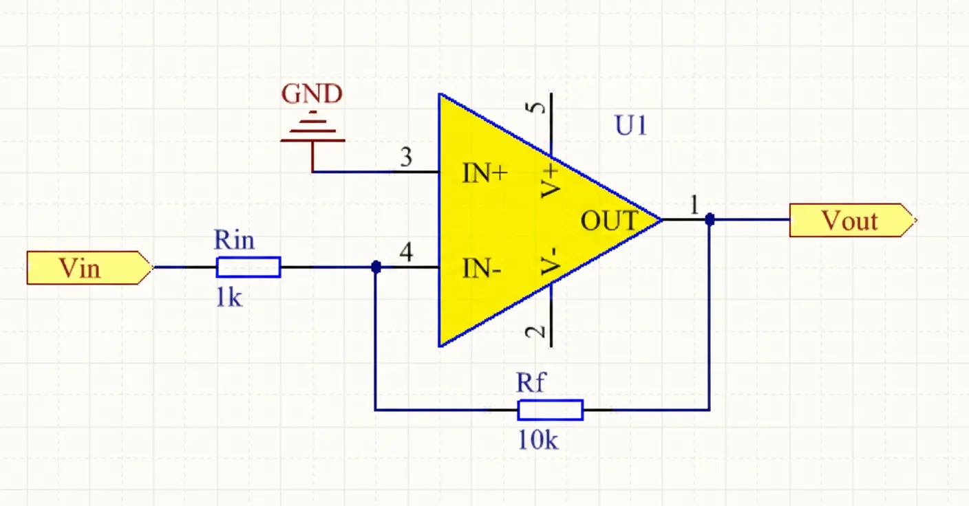
An inverting amplifier using an op amp inverts and amplifies the input signal. The ideal closed-loop gain is:
Vout = -Vin * Rf / Rin
For example, with Rf = 10 kΩ and Rin = 1 kΩ the expected gain is 10. Remember this result for the following analysis.
Why the Input Impedance Is Low
Using the op amp's virtual short and virtual ground properties: the noninverting input is at ground potential, so the inverting input is also at approximately 0 V. The right side of Rin is effectively at 0 V, making the input impedance seen by the source equal to Rin. Thus the input impedance of the inverting amplifier equals Rin, which in this example is 1 kΩ.
Effect of Source Internal Resistance
Most practical signal sources are not ideal voltage sources and include an internal resistance, which we denote Rz. If the source internal resistance is, for example, 1 kΩ, then Rz and Rin are in series from the perspective of the amplifier input. The effective input to the amplifier is reduced, and the closed-loop gain becomes:
Vout = -Vin * Rf / (Rz + Rin)
With Rf = 10 kΩ, Rin = 1 kΩ and Rz = 1 kΩ, the actual gain is 10 kΩ / (1 kΩ + 1 kΩ) = 5, not the expected 10. If different sources with different internal resistances drive the same amplifier, the gain will vary accordingly.
Polarity of the Output
Because the inverting input node is at virtual ground, current through Rin flows such that the output voltage is negative relative to ground for a positive input, which explains the negative sign in the gain formula. The current directions in the circuit allow straightforward derivation of the formula.
Conclusion
The low input impedance inherent to the inverting configuration can cause significant gain error or instability when driven by sources with nonnegligible internal resistance. In a past project this effect caused the op amp output to be very unstable. Designers should account for source impedance when choosing the amplifier topology or include buffering to isolate the source from the amplifier input.