ALLPCB


Over time, many fixed circuit design modules have become standard practice. Remembering these modules improves design efficiency and reduces errors. The main modules covered here include power, storage, display, and external interface modules.
- Power module, storage module, display module, external interface module
1. Power
Power is the lifeblood of a system and directly affects product stability and certification. Key practices include:
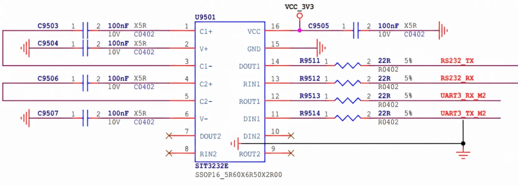
- Prefer a pi filter topology and add a 10 uH inductor. Place a 0.1 uF bypass capacitor on each chip power pin.
- Use a varistor or transient suppression diode to suppress surges.
- Keep analog and digital grounds separate; separate high-current and low-current return loops. Use ferrite beads or zero-ohm resistors to isolate.
- Design with margin to avoid power IC overheating. Apply a heatsink when power dissipation reaches about 50% of the rated value.
2. IO: pull-ups and drive capability
Pull up input IOs as required. For output IOs, verify the drive capability to ensure proper interfacing and signal integrity.
3. Avoid connecting a capacitor directly to an op amp output
In DC signal amplification, placing a decoupling capacitor directly on an op amp output to reduce noise is unsafe. When a step input occurs or during power-up, the op amp output current can spike and the capacitor alters loop phase, which may cause oscillation. The correct approach is to form an RC network: insert a series resistor at the op amp output, then place the decoupling capacitor to ground. This reduces instantaneous output current and preserves loop phase margin, avoiding oscillation.
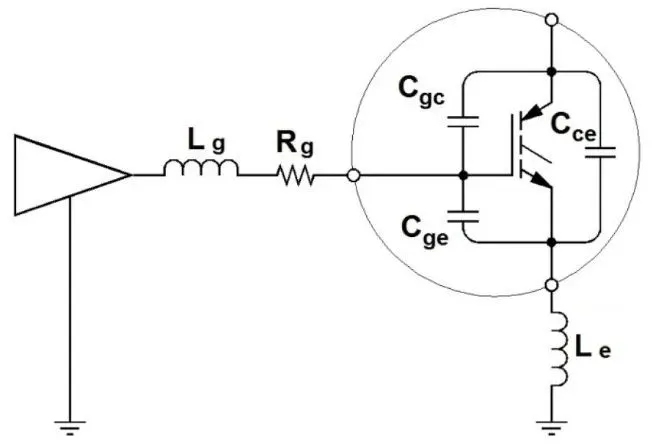
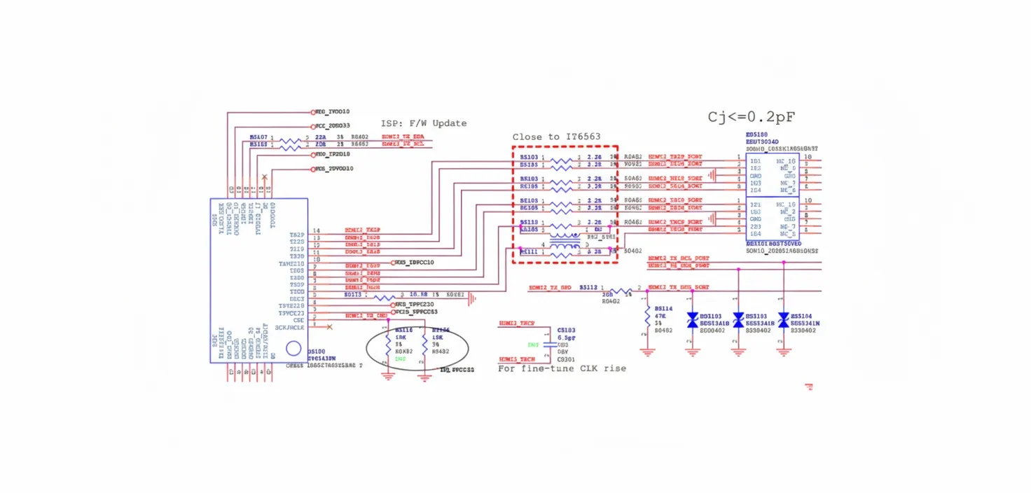
4. High-speed IO termination and differential matching
For long high-speed traces, use a 33 ohm series resistor to suppress reflections. At the receiver, add a differential termination resistor equal to the differential impedance to improve signal quality.
5. Level matching and ground return planning
When boards connect, signals or supply currents sent from board A to board B produce equal return currents in the ground plane per Kirchhoff's current law. Return currents follow the lowest impedance path. Therefore, ensure sufficient ground pins at interfaces to lower impedance and reduce ground noise. Analyze return current loops, especially high-current paths, and adjust ground plane or traces to guide currents through low-impedance routes to minimize impact on sensitive signals.
6. Switching device overshoot
For switching devices, evaluate whether measures are needed to prevent transistor switching overshoot, such as snubbers, RC dampers, or controlled slew-rate techniques.
7. Testable single boards
Design each board so it has a testable circuit and can independently complete functional tests.
8. Test points
Add test points on the PCB. As a rule, make test points as small and short as practical while meeting test equipment requirements. Include test points for important signals and ground references.
9. Avoid high-frequency interference
Reduce high-frequency electromagnetic interference and crosstalk by increasing spacing between high-speed and analog signals, or adding ground guard or shunt traces adjacent to analog traces. Pay attention to noise coupling between digital and analog grounds and take measures to isolate or control it.
If schematics and PCB designs consistently check these points, the likelihood of successful designs increases, the number of revisions is reduced, and design cycles shorten. The above summarizes nine essential circuit modules for hardware engineers; mastering these modules helps complete designs and iterations more quickly.