 ALLPCB


Introduction
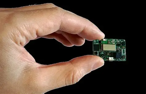
Space-constrained IoT devices, such as wearable sensors and remote environmental monitors, demand printed circuit boards (PCBs) that pack maximum functionality into minimal footprints. Engineers face the dual challenge of achieving the smallest possible PCB for IoT sensors while maintaining reliability, signal integrity, and power efficiency. As IoT deployments expand into smart homes, agriculture, and healthcare, compact designs reduce material costs, simplify enclosures, and enable seamless integration into tight spaces. However, shrinking PCB size introduces complexities like thermal management, electromagnetic interference, and manufacturing yields. This article explores strategies for optimizing PCB dimensions, focusing on component selection for miniaturization, antenna integration for IoT devices, power efficiency considerations in compact designs, and balancing size and functionality. By applying structured engineering approaches, designers can create robust solutions that meet performance goals without compromising manufacturability.
Why PCB Miniaturization Matters for IoT Applications
Miniaturization directly impacts the viability of IoT devices in real-world scenarios where size dictates deployment feasibility. For instance, battery-powered nodes in structural health monitoring require boards under a few square centimeters to fit within existing infrastructure. Smaller PCBs lower overall system weight, which is critical for drones or implantable medical devices, and reduce assembly time during high-volume production. Yet, aggressive size reduction risks signal degradation, higher failure rates, and elevated costs from specialized processes. Industry trends show a shift toward high-density interconnect (HDI) structures to achieve the smallest possible PCB for IoT sensors, enabling feature-rich designs in constrained volumes. Understanding these trade-offs ensures engineers prioritize aspects like power efficiency considerations in compact designs from the outset.
The relevance extends to lifecycle costs, as compact boards facilitate easier recycling and compliance with sustainability goals. Electrical engineers must evaluate how size influences electromagnetic compatibility and mechanical stress during operation. In essence, effective miniaturization aligns device performance with practical constraints, fostering innovation in edge computing and wireless networks.
Core Technical Principles of PCB Size Optimization
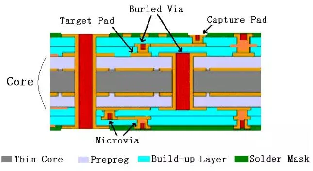
PCB size optimization begins with substrate selection and layer stacking to maximize routing density without excessive via usage. Thinner cores and build-up layers in HDI configurations allow trace widths below 50 microns, supporting finer pitch components essential for compact IoT layouts. Microvias and blind vias reduce board thickness, enabling stacked designs that fit IoT sensors into millimeter-scale enclosures. Signal integrity principles dictate controlled impedance traces, even in dense areas, to prevent crosstalk in high-speed interfaces like SPI or I2C. Thermal dissipation follows basic conduction laws, where smaller areas necessitate copper pours or embedded heat spreaders to avoid hotspots.
Power distribution networks must account for voltage drops in miniaturized traces, often requiring wider planes or decoupling capacitors placed strategically near ICs. Antenna integration for IoT devices relies on clearance areas and ground planes that maintain radiation efficiency despite size limits. Adhering to IPC-6012E qualification standards ensures these dense structures withstand environmental stresses like vibration and humidity. Overall, these principles form the foundation for achieving the smallest possible PCB for IoT sensors while upholding electrical performance.
Component Selection Strategies for Miniaturization
Selecting components for miniaturization involves prioritizing packages with the lowest profiles and smallest footprints compatible with IoT functionality. Passive elements like resistors and capacitors in 01005 or 0201 sizes occupy minimal space, allowing denser placement without sacrificing capacitance or resistance values. Integrated circuits in wafer-level chip-scale packages (WLCSP) or quad flat no-lead (QFN) formats reduce height to under 0.5 mm, ideal for power efficiency considerations in compact designs. Microcontrollers with integrated RF transceivers, such as those supporting Bluetooth Low Energy, consolidate functions onto a single die, shrinking overall board area.
Engineers must verify component reliability through JEDEC moisture sensitivity classifications to prevent reflow defects in small assemblies. Active devices like sensors demand low-power variants with integrated filters to minimize external support circuitry. Balancing component pitch with solder paste application ensures high yields; finer pitches below 0.3 mm require laser-cut stencils. By cataloging options based on electrical specs and thermal limits, designers systematically downsize without functionality loss.
This approach extends to power management ICs, where buck converters in tiny packages deliver efficient regulation for battery life extension. Practical selection matrices help compare trade-offs, such as cost versus performance, guiding decisions for volume production.
Antenna Integration Challenges in Compact IoT PCBs
Antenna integration for IoT devices poses unique hurdles in size-optimized PCBs, as radiating elements need sufficient ground plane area for optimal gain. Chip antennas offer the smallest footprints, measuring mere millimeters, but demand precise matching networks tuned to 2.4 GHz or sub-GHz bands. PCB trace antennas, like inverted-F types, leverage board edges but require keep-out zones that conflict with dense routing. In the smallest possible PCB for IoT sensors, engineers balance feedline length with impedance control to achieve return loss below -10 dB.
Balancing size and functionality means simulating near-field effects, where nearby components detune the antenna, necessitating shielding or relocation. Power efficiency considerations in compact designs amplify this, as mismatched antennas increase transmit current draw. Ground plane segmentation isolates RF sections, following basic isolation rules to minimize substrate losses. Compliance with IEC electromagnetic compatibility standards validates these integrations under operational conditions.
Testing involves over-the-air measurements in anechoic chambers to quantify efficiency drops from size constraints. Iterative design refines layouts, often prioritizing meander-line antennas for sub-1 cm boards.
Power Efficiency Considerations in Compact Designs
Power efficiency in compact designs hinges on minimizing quiescent currents and optimizing DC paths across the PCB. Low-dropout regulators and sleep-mode microcontrollers extend battery life in intermittent IoT operations. Trace resistance calculations guide plane sizing; narrower traces in small boards elevate IR drops, demanding higher supply voltages or parallel routing. Decoupling strategies place capacitors within 1 mm of pins to suppress noise, critical for analog sensors.
Energy harvesting interfaces, like solar or kinetic, integrate via efficient DC-DC converters tailored for micro-power levels. Thermal modeling predicts junction temperatures, as dense packing raises self-heating despite low dissipation. Engineers apply these principles to achieve microampere standby modes, directly supporting the smallest possible PCB for IoT sensors.
Balancing Size and Functionality: Key Trade-Offs
Balancing size and functionality requires holistic design reviews encompassing signal, power, and mechanical domains. Signal integrity tools verify eye diagrams for high-speed lines squeezed into tiny vias. Manufacturability assessments per IPC-A-600K acceptability criteria flag defects like insufficient annular rings in microvias. Cost modeling weighs HDI premiums against volume savings from smaller boards.
Reliability testing simulates field stresses, ensuring compact assemblies endure thermal cycling. Firmware optimizations complement hardware by duty-cycling peripherals, easing size pressures. This equilibrium yields deployable IoT solutions.
Best Practices for Implementation
Start with requirements capture, defining must-have features before layout. Employ hierarchical design flows: partition RF, digital, and analog zones early. Prototype iterations validate assumptions, focusing on yield data from assembly partners. Documentation includes stack-up drawings and fab notes for reproducibility.
Conclusion
Optimizing PCB size for space-constrained IoT devices demands integrated strategies across component selection for miniaturization, antenna integration for IoT devices, and power efficiency considerations in compact designs. By mastering technical principles and trade-offs, engineers achieve the smallest possible PCB for IoT sensors without sacrificing reliability. Balancing size and functionality ensures scalable, efficient products ready for diverse applications. Adopting these practices positions designs for success in a miniaturization-driven era.
FAQs
Q1: What factors determine the smallest possible PCB for IoT sensors?
A1: Component footprints, via densities, and HDI layer counts primarily dictate minimum size. Engineers select 01005 passives and WLCSP ICs while ensuring routing feasibility for signals and power. Antenna keep-outs and thermal vias add constraints, but simulations optimize layouts. Adhering to standards like IPC-6012E maintains quality in these ultra-compact boards.
Q2: How do power efficiency considerations in compact designs affect PCB size?
A2: Compact designs prioritize low-power components to fit efficient regulators and minimal decoupling. Narrow traces increase resistance, so wider power planes or multi-layer stacks balance this. Sleep modes reduce active area needs, enabling smaller footprints. Balancing size and functionality here extends battery life without expanding the board.
Q3: What are best practices for antenna integration for IoT devices on small PCBs?
A3: Use chip or PCB-trace antennas with dedicated ground planes for efficiency. Tune matching networks via simulation to counter detuning from nearby components. Allocate 10-20% board area for RF isolation. Test radiated performance early to refine layouts, ensuring reliable wireless links in space-constrained IoT setups.
Q4: How to approach component selection for miniaturization in IoT projects?
A4: Catalog components by size, power, and package type, favoring QFN or BGA for density. Verify JEDEC classifications for assembly compatibility. Prioritize multi-function ICs to reduce part count. Prototype to confirm signal integrity, iteratively shrinking while preserving functionality.


