 ALLPCB


If you're new to printed circuit board (PCB) inspection and wondering how to ensure your boards are free of defects, manual PCB inspection is a great starting point. This process involves visually checking a PCB for issues like soldering defects, component misalignment, or physical damage using basic tools and techniques. In this comprehensive guide, we'll walk you through the essentials of manual PCB inspection, visual PCB inspection methods, the best PCB inspection tools, and tips for effective PCB soldering inspection. Whether you're a hobbyist or a budding engineer, this step-by-step tutorial will help you master the art of inspecting PCBs with confidence.
Why Manual PCB Inspection Matters for Beginners
Manual PCB inspection is often the first line of defense in ensuring the quality of a circuit board. Before advanced automated systems or electrical testing come into play, a thorough visual check can catch obvious defects that could lead to failures down the line. For beginners, mastering this skill is crucial because it builds a foundational understanding of PCB design and assembly issues. Plus, it’s cost-effective since it requires minimal investment in tools compared to automated inspection systems.
By focusing on visual PCB inspection, you can identify problems like poor solder joints, missing components, or damaged traces. According to industry data, up to 70% of PCB defects can be spotted through manual inspection before they cause functional issues. This makes it an essential skill for anyone working with electronics.
What Is Manual PCB Inspection?
Manual PCB inspection, often referred to as visual PCB inspection, is the process of examining a printed circuit board with the naked eye or with the help of simple magnification tools. The goal is to identify physical or assembly defects without relying on complex machinery or electrical testing. This method is widely used in small-scale production, prototyping, or by hobbyists who may not have access to advanced equipment.
During a manual inspection, you’re looking for issues such as:
- Incorrect or missing components
- Poor soldering quality (e.g., cold joints, excess solder, or bridges)
- Damaged or misaligned traces and pads
- Physical damage like cracks or scratches on the board
For beginners, this process is a hands-on way to learn about PCB assembly and quality control. It also helps in troubleshooting issues before powering up the board, preventing potential damage to components.
Essential PCB Inspection Tools for Beginners
To perform an effective manual PCB inspection, you don’t need expensive equipment. Here are the basic PCB inspection tools every beginner should have:
- Magnifying Glass or Loupe: A 5x to 10x magnification tool helps you see tiny details like solder joints or small cracks that are invisible to the naked eye.
- LED Desk Lamp or Ring Light: Good lighting is critical for spotting defects. A bright, focused light source with adjustable intensity ensures you don’t miss anything.
- Tweezers: Precision tweezers are useful for handling small components or gently probing solder joints to check for loose connections.
- Multimeter: While not strictly for visual inspection, a multimeter can help verify continuity in traces or check for shorts after a visual check.
- Inspection Checklist: A printed or digital checklist ensures you cover all critical areas during inspection, especially as a beginner.
These tools are affordable and widely available, making them ideal for anyone starting with manual PCB inspection. Investing in quality tools can save time and improve accuracy. For instance, a magnifying glass with built-in LED lighting can cost as little as $10 but significantly enhances visibility.
Step-by-Step Guide to Manual PCB Inspection
Now that you have the tools, let’s dive into a detailed, step-by-step process for conducting a manual PCB inspection. Follow these steps to ensure you don’t miss any critical defects.
Step 1: Prepare Your Workspace
Start by setting up a clean, well-lit workspace. Remove any clutter that could interfere with your inspection. Use an anti-static mat or wrist strap to prevent electrostatic discharge (ESD) from damaging sensitive components. Place your PCB on a flat surface under good lighting, and keep your tools within reach.
Step 2: Perform an Initial Visual Check
Begin with a quick overall scan of the PCB without magnification. Look for obvious issues like missing components, visible cracks, or burnt areas. Hold the board at different angles under the light to catch reflections that might reveal scratches or uneven surfaces. This initial check helps you identify major defects before diving into detailed inspection.
Step 3: Inspect Component Placement
Using a magnifying glass, check if all components are placed correctly according to the PCB design or schematic. Ensure that:
- Components match the markings on the silkscreen layer.
- Polarized components like capacitors and diodes are oriented correctly.
- No components are missing or misaligned.
Misplaced components can cause circuit failure, so take your time with this step.
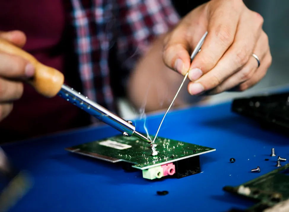
Step 4: Focus on PCB Soldering Inspection
Soldering defects are among the most common issues in PCB assembly. During PCB soldering inspection, look for the following:
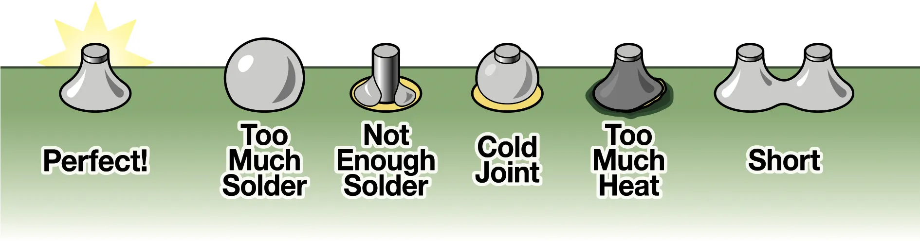
- Cold Solder Joints: These appear dull and grainy rather than shiny and smooth. They can cause intermittent connections.
- Solder Bridges: Excess solder connecting two adjacent pads or pins, which can create short circuits.
- Insufficient Solder: Joints with too little solder may not provide a strong connection, leading to failures under stress.
- Excess Flux Residue: Leftover flux can attract dust or cause corrosion over time if not cleaned properly.
A good solder joint should form a concave shape, covering the pad and pin evenly. If you spot a defect, note it down for rework. For example, a cold joint on a resistor lead might measure higher resistance (e.g., above 1 ohm) when tested with a multimeter, indicating a poor connection.
Step 5: Examine Traces and Pads
Inspect the copper traces and pads for any signs of damage. Look for:
- Cracks or breaks in traces that could interrupt signal flow. A broken trace might result in an open circuit, causing a section of the board to fail.
- Lifted pads, often caused by excessive heat during soldering.
- Scratches or corrosion on the surface that might affect conductivity.
If you suspect a trace issue, use a multimeter to check for continuity. A reading of infinite resistance indicates a break in the circuit.
Step 6: Check for Physical Damage
Finally, look for any physical damage to the PCB itself. This includes cracks in the substrate, warped areas, or chipped edges. Physical damage can compromise the structural integrity of the board, especially in applications subject to vibration or mechanical stress.
Step 7: Document Findings and Plan Rework
Record any defects you find during the inspection. Use a checklist or take photos to document issues for future reference. If defects are found, decide whether they can be fixed through rework (e.g., re-soldering a joint) or if the board needs to be discarded. For beginners, it’s helpful to keep a log of common issues to learn from mistakes over time.
Common Defects to Watch for During Visual PCB Inspection
As a beginner, it’s important to familiarize yourself with the most common defects encountered during visual PCB inspection. Here are some frequent issues and how to spot them:
- Tombstoning: A component stands upright on one end due to uneven soldering. This often happens with small resistors or capacitors and looks like a tombstone.
- Burn Marks: Darkened areas on the board may indicate overheating during soldering or a short circuit during testing.
- Misaligned Components: Components not seated flush against the board can cause poor connections or mechanical stress.
- Solder Splashes: Small blobs of solder scattered across the board can create unintended connections.
By learning to recognize these defects, you’ll improve your inspection accuracy and prevent costly errors in your projects.
Tips for Effective Manual PCB Inspection
To make your manual PCB inspection process smoother and more effective, consider these practical tips:
- Take Breaks: Staring at a PCB for long periods can strain your eyes. Take short breaks every 20-30 minutes to maintain focus.
- Use a Reference: Keep the PCB schematic or assembly drawing nearby to cross-check component placement and values.
- Work Systematically: Inspect the board in sections (e.g., top to bottom, left to right) to ensure you don’t miss any areas.
- Practice Patience: Rushing through an inspection can lead to overlooked defects. Take your time, especially as a beginner.
- Learn from Experience: Each inspection is a learning opportunity. Over time, you’ll develop an eye for spotting issues quickly.
Limitations of Manual PCB Inspection
While manual PCB inspection is a valuable skill, it has its limitations. It’s not suitable for detecting internal defects like hidden shorts or issues in multilayer boards. For high-volume production, automated optical inspection (AOI) systems are more efficient, as they can process hundreds of boards per hour with greater accuracy. Additionally, human error can play a role in manual inspections, especially for beginners who are still learning.
For critical applications, combining manual inspection with electrical testing (like in-circuit testing) ensures a higher level of quality control. However, for small projects or learning purposes, manual inspection remains an excellent starting point.
Enhancing Your Skills in PCB Soldering Inspection
Since soldering issues are a major focus of PCB inspection, improving your soldering skills can reduce defects from the start. Here are a few pointers to enhance your PCB soldering inspection process:
- Use the correct soldering iron tip and temperature. For most PCB work, a temperature of 300°C (572°F) is ideal for lead-free solder.
- Apply solder sparingly to avoid bridges. A good rule of thumb is to use just enough to form a small fillet around the joint.
- Clean the board after soldering to remove flux residue, which can obscure defects during inspection.
By refining your soldering technique, you’ll make the inspection process easier and more effective.
Conclusion: Building Confidence in Manual PCB Inspection
Mastering manual PCB inspection is a fundamental skill for anyone working with electronics. By following the step-by-step guide outlined above, using the right PCB inspection tools, and paying close attention during visual PCB inspection and PCB soldering inspection, you can catch defects early and ensure the reliability of your projects. While it takes practice to develop a keen eye for detail, the effort pays off in the form of better-quality boards and fewer failures.
Start small, be patient, and use each inspection as a chance to learn. With time, you’ll gain the confidence to spot issues quickly and even prevent them during assembly. Remember, every expert started as a beginner, and with dedication, you can become proficient in manual PCB inspection too.


