 ALLPCB


If you're looking to understand the factors behind PCB cost and the role of PCB imaging in the fabrication process, you're in the right place. PCB cost is influenced by materials, design complexity, layer count, and manufacturing processes, typically ranging from a few cents to hundreds of dollars per board depending on specifications. PCB imaging, a critical step in fabrication, involves transferring circuit designs onto the board using techniques like photolithography to ensure precision. In this comprehensive guide, we'll dive deep into the elements that drive PCB costs, the intricacies of PCB imaging, and how these aspects impact the overall production of printed circuit boards. Whether you're an engineer, designer, or hobbyist, this blog will provide actionable insights to help you navigate the world of PCB fabrication.
What Drives PCB Cost in Fabrication?
The cost of a printed circuit board (PCB) can vary widely based on several key factors. Understanding these elements can help you make informed decisions during the design and manufacturing process to optimize both quality and budget. Let's break down the primary drivers of PCB cost, focusing on material choices, design complexity, and production volume.
Material Costs in PCB Fabrication
The choice of materials is one of the biggest factors affecting PCB cost. The substrate, which forms the base of the board, and the conductive layers, typically made of copper, are the primary materials to consider. Here are some common materials and their impact on cost:
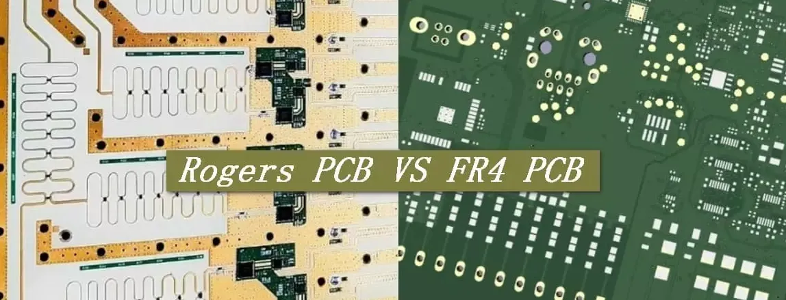
- FR-4: This is the most common substrate material, made of woven fiberglass and epoxy resin. It's cost-effective and suitable for most standard applications, with prices often ranging from $0.50 to $2 per square foot for basic boards.
- High-Frequency Materials: For applications requiring high-speed signal transmission, such as RF or microwave circuits, specialized materials like PTFE or ceramic-filled laminates are used. These can increase costs significantly, often exceeding $5 per square foot.
- Copper Thickness: The amount of copper used, measured in ounces per square foot (e.g., 1 oz or 2 oz), also affects cost. Thicker copper layers, needed for high-current applications, can add 10-20% to the material cost.
Beyond the substrate and copper, other materials like solder mask (a protective layer) and surface finishes (e.g., HASL, ENIG) contribute to the overall expense. For instance, opting for a gold finish for better conductivity and corrosion resistance can add $1-3 per board compared to cheaper alternatives.
Design Complexity and Layer Count
The complexity of your PCB design directly impacts fabrication costs. A simple single-layer board used in basic electronics will cost much less than a multi-layer board designed for complex devices like smartphones or medical equipment.
- Number of Layers: Each additional layer increases the cost due to added materials and manufacturing steps. A 2-layer board might cost around $1-2 per unit in small batches, while a 6-layer board could jump to $5-10 per unit.
- Trace and Space: Smaller trace widths and spacing, often required for high-density designs, demand advanced manufacturing precision, driving up costs by 15-30%. For example, traces below 6 mils (0.006 inches) often require specialized equipment.
- Vias and Drill Holes: The number and type of vias (connections between layers) also play a role. Microvias or blind vias, used in high-density interconnect (HDI) boards, can increase costs by 20-40% compared to standard through-hole vias.
If you're working on a high-speed design, impedance control becomes crucial. Achieving specific impedance values, such as 50 ohms for RF signals, may require tighter manufacturing tolerances, adding to the expense.
Production Volume and Economies of Scale
The quantity of boards you order significantly affects the per-unit cost. Manufacturing setups involve fixed costs for tooling and setup, so larger orders spread these expenses across more units, reducing the cost per board.
- Prototyping: Small runs or prototypes (1-10 boards) often cost $10-50 per board due to setup fees.
- Medium Volume: Ordering 100-500 boards can drop the price to $2-5 per board as setup costs are distributed.
- High Volume: For orders of 1,000 or more, costs can fall below $1 per board for simple designs.
Planning your production volume carefully can save significant amounts, especially if you can combine multiple designs into a single production run to maximize panel usage.
The Role of PCB Imaging in Fabrication
PCB imaging is a critical step in the fabrication process, where the circuit design is transferred onto the board. This process ensures that the copper traces, pads, and other features are accurately placed according to the design specifications. Let's explore what PCB imaging involves, the technologies used, and why it matters for the quality of the final product.
What Is PCB Imaging?
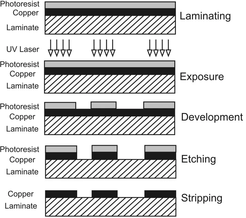
PCB imaging, often referred to as photolithography in traditional manufacturing, is the process of creating a pattern of the circuit design on the board's surface. It starts with a photosensitive layer, called photoresist, applied to the copper-clad board. The design is then projected or printed onto this layer using light or laser technology, hardening or softening specific areas of the photoresist. After exposure, the unneeded photoresist is washed away, leaving behind the pattern for etching, where unprotected copper is removed to form the circuit traces.
This step is crucial because even a small error in imaging can lead to misaligned traces, short circuits, or open connections, rendering the board unusable. For high-speed designs, precise imaging ensures signal integrity by maintaining consistent trace widths and spacing, which directly affect impedance values (e.g., maintaining a 50-ohm impedance for RF applications).
Technologies Used in PCB Imaging
Several imaging technologies are used in PCB fabrication, each suited to different levels of precision and production needs:
- Photolithography: The traditional method uses UV light and a photomask (a film or glass plate with the circuit pattern) to expose the photoresist. It's cost-effective for medium to high-volume production but less ideal for quick-turn prototypes due to the time needed to create masks.
- Laser Direct Imaging (LDI): This modern technique uses a laser to directly draw the circuit pattern onto the photoresist, eliminating the need for a photomask. LDI offers higher precision, achieving trace widths as small as 2 mils (0.002 inches), and is ideal for HDI boards and prototypes. However, it can increase costs by 10-20% compared to traditional methods.
- Inkjet Printing: An emerging technology for low-volume or prototype boards, inkjet printing deposits etch-resistant ink directly onto the board to form the pattern. While it's faster for small runs, it lacks the precision of LDI for fine-pitch designs.
The choice of imaging technology depends on the design requirements and budget. For instance, if you're designing a board with fine traces below 4 mils, investing in LDI might be necessary to ensure accuracy.
Impact of PCB Imaging on Cost and Quality
PCB imaging not only affects the quality of the board but also influences the overall cost of fabrication. High-precision imaging methods like LDI, while more expensive, reduce the risk of defects and rework, which can save money in the long run, especially for complex designs. On the other hand, opting for cheaper imaging methods might lower upfront costs but could lead to higher failure rates during testing or in the field.
For example, a misalignment in imaging could cause a trace to deviate by just 1 mil, potentially disrupting a high-speed signal traveling at 3 GHz, leading to signal loss or crosstalk. Investing in better imaging technology upfront ensures reliability, especially for critical applications in aerospace or medical devices.
How Board Components Influence PCB Cost
While material and imaging costs are significant, the components mounted on the PCB during assembly also play a role in the overall expense. The type, quantity, and availability of components can add up quickly, especially for complex designs.
Component Selection and Cost
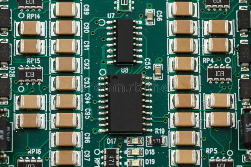
The components used on a PCB, such as resistors, capacitors, integrated circuits (ICs), and connectors, vary widely in price based on their specifications and sourcing.
- Basic Components: Simple components like resistors and capacitors might cost just a few cents each, but in large quantities, even these small costs add up. For a board with 100 components, this could mean $5-10 in total.
- Specialized ICs: High-performance microcontrollers or RF chips can cost $10-50 or more per unit, significantly increasing the assembly cost for each board.
- Availability: Components that are out of stock or obsolete often require sourcing from secondary markets, driving up costs by 50-100% or more due to scarcity.
Designing with commonly available, standard components can help keep costs down. Additionally, using surface-mount technology (SMT) components instead of through-hole ones can reduce assembly costs due to faster automated placement, though SMT requires precise imaging and soldering processes.
Assembly and Testing Costs
Once components are selected, the assembly process—soldering components onto the board—adds another layer of cost. Automated assembly for SMT components is generally cheaper per unit, often costing $0.01-0.05 per component placement, but manual assembly for prototypes or through-hole components can cost $0.50-1 per placement.
Testing is another critical step that impacts cost. Functional testing to verify signal integrity (e.g., ensuring a 1 GHz signal propagates without loss) or in-circuit testing to check component values can add $1-5 per board, depending on the complexity. Skipping testing might save money upfront but risks costly failures later.
Balancing Cost and Quality in PCB Fabrication
Finding the right balance between cost and quality is essential in PCB fabrication. Here are some practical tips to optimize your project:
- Simplify Designs: Reduce layer count and avoid unnecessarily tight tolerances unless required for performance. For example, if a 10-mil trace width works for your design, don't specify 6 mils just for aesthetics.
- Choose Materials Wisely: Use standard materials like FR-4 for non-critical applications to keep costs down, reserving high-frequency materials for designs where signal speed (e.g., above 1 GHz) is critical.
- Plan Production Volume: Order in larger batches to benefit from economies of scale, and consider panelizing multiple designs to maximize board usage.
- Invest in Imaging Precision: For complex or high-speed designs, allocate budget for advanced imaging technologies to avoid costly defects and rework.
By understanding the interplay between PCB cost factors and the importance of imaging, you can make strategic decisions that ensure both affordability and reliability for your projects.
Conclusion
Navigating the world of PCB fabrication involves a deep understanding of cost drivers like material selection, design complexity, and production volume, as well as critical processes like PCB imaging. From choosing cost-effective materials to investing in precise imaging technologies for accurate trace placement, every decision impacts the final cost and quality of your board. Whether you're designing a simple prototype or a complex multi-layer board for high-speed applications, keeping these factors in mind can help you achieve the best results within your budget. With the insights provided in this guide, you're better equipped to tackle your next PCB project with confidence and efficiency.


