ALLPCB


Electroless Nickel Immersion Gold (ENIG) is a popular surface finish for printed circuit boards (PCBs) due to its excellent solderability and corrosion resistance. However, a common issue known as "black pad" can compromise the reliability of solder joints, leading to failures in electronic assemblies. If you're a PCB manufacturer looking to understand and resolve ENIG black pad issues, you're in the right place. This guide will dive deep into ENIG black pad causes, ENIG black pad prevention, ENIG black pad detection, PCB surface finish reliability, and solder joint failure analysis to help you ensure high-quality production.
In the sections below, we'll explore the root causes of black pad, provide actionable steps to prevent it, and share methods to detect and address this defect. Whether you're dealing with field failures or aiming to improve manufacturing processes, this practical guide offers the insights you need to maintain reliable PCB performance.
What Is ENIG Black Pad and Why Does It Matter?
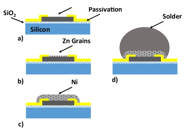
ENIG black pad is a defect that occurs during the application of the ENIG surface finish on PCBs. It appears as a dark, corroded layer on the nickel surface beneath the thin gold layer, often invisible to the naked eye until soldering issues arise. This corrosion weakens the bond between the nickel layer and the solder, resulting in brittle solder joints that can crack or fail under stress. For PCB manufacturers, black pad defects can lead to costly rework, customer dissatisfaction, and compromised product reliability, especially in high-stakes industries like automotive or aerospace.
The impact of black pad is significant because it directly affects PCB surface finish reliability. A reliable surface finish ensures strong solder joints, which are critical for the electrical and mechanical performance of a PCB. When black pad occurs, it undermines this reliability, often leading to failures that are difficult to detect until the assembly stage or, worse, after deployment in the field.
ENIG Black Pad Causes: Understanding the Root Issues
To effectively address black pad, it's essential to understand what causes it. The defect typically arises during the ENIG plating process due to a combination of chemical and environmental factors. Below are the primary ENIG black pad causes:
- Galvanic Corrosion During Gold Plating: The immersion gold process can lead to galvanic hyper-corrosion of the nickel layer if the chemical bath is not properly controlled. This corrosion creates a defective interface that appears as black pad, weakening solder joint adhesion.
- Improper Bath Chemistry: Imbalances in pH, temperature, or chemical composition of the plating baths can accelerate nickel corrosion. For instance, a gold bath with excessive acidity (pH below 4.0) can attack the nickel layer, increasing the risk of black pad formation.
- Contamination: Contaminants such as organic residues or metallic impurities in the plating solution can interfere with the uniform deposition of gold, leading to uneven nickel exposure and subsequent corrosion.
- Excessive Phosphorus Content: The electroless nickel layer often contains phosphorus as a byproduct of the plating process. If the phosphorus content exceeds 10-11% by weight, it can make the nickel more prone to corrosion during the gold immersion step.
- Poor Process Control: Inconsistent immersion times, inadequate rinsing between plating steps, or insufficient agitation in the bath can all contribute to black pad formation.
By identifying these root causes, manufacturers can target specific areas of the ENIG process for improvement. Addressing these issues early is key to maintaining PCB surface finish reliability and preventing costly defects.
ENIG Black Pad Prevention: Best Practices for Manufacturers
Preventing black pad is far more effective than dealing with it after it occurs. By implementing strict process controls and best practices, manufacturers can significantly reduce the risk of this defect. Here are actionable strategies for ENIG black pad prevention:
- Optimize Bath Chemistry: Regularly monitor and adjust the pH, temperature, and chemical composition of the nickel and gold plating baths. Maintain the gold bath pH between 4.5 and 5.5 to minimize nickel corrosion. Use analytical testing to ensure phosphorus levels in the nickel layer stay between 7-9% by weight.
- Enhance Process Control: Standardize immersion times and ensure thorough rinsing between plating steps to remove residual chemicals. For example, limit gold immersion time to 8-12 minutes to avoid excessive nickel exposure.
- Use High-Purity Materials: Source high-quality plating chemicals and ensure that the plating solutions are free from organic or metallic contaminants. Filtration systems can help maintain bath purity.
- Implement Pre-Treatment Steps: Clean and activate the copper surface before nickel plating to ensure uniform deposition. A micro-etching step with a controlled etch rate of 20-40 microinches can improve adhesion and reduce defects.
- Consider Alternative Finishes for High-Risk Applications: For applications where black pad risk must be minimized, consider using Electroless Nickel Electroless Palladium Immersion Gold (ENEPIG). This finish adds a palladium layer between nickel and gold, reducing the risk of corrosion, though it comes at a higher cost.
- Train Staff and Audit Processes: Ensure that operators are trained in proper plating techniques and conduct regular audits of the ENIG process to identify and correct deviations.
By adopting these prevention strategies, manufacturers can enhance PCB surface finish reliability and avoid the headaches associated with black pad defects. Consistency and attention to detail are critical in achieving defect-free ENIG finishes.
ENIG Black Pad Detection: Identifying Issues Early
Detecting black pad early in the manufacturing process can save significant time and resources. Since the defect is often hidden beneath the gold layer, specialized techniques are required for ENIG black pad detection. Here are some effective methods:
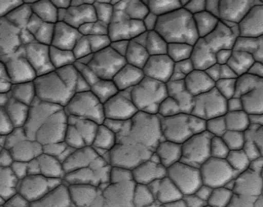
- Visual Inspection Under Magnification: While black pad is not always visible to the naked eye, high-magnification microscopes (50x or higher) can reveal dark, corroded areas on the nickel surface after removing the gold layer with a mild etchant.
- High-Speed Pull Testing: Perform pull tests on soldered joints to expose the pad surface. A brittle fracture at the nickel-solder interface often indicates black pad. Testing should achieve a pull strength of at least 1.5 kgf for reliable joints.
- Scanning Electron Microscopy (SEM) and Energy-Dispersive X-Ray Analysis (EDX): These advanced techniques can analyze the microstructure and chemical composition of the ENIG layer. SEM can reveal corrosion patterns, while EDX can detect high phosphorus content or other anomalies at the interface.
- Cross-Sectional Analysis: Use a focused-ion beam (FIB) to create precise cross-sections of the ENIG layer for detailed examination. This method can identify corrosion depth and structural defects, often revealing black pad layers as thin as 0.1 micrometers.
- Solderability Testing: Conduct solderability tests using industry standards like IPC J-STD-003. Poor wetting or de-wetting during soldering can be an early indicator of black pad issues.
Early detection allows manufacturers to address black pad before it leads to widespread failures, preserving the integrity of their products and maintaining customer trust.
Solder Joint Failure Analysis: Diagnosing Black Pad Impact
When black pad goes undetected, it often results in solder joint failures that can compromise the functionality of a PCB. Conducting a thorough solder joint failure analysis is crucial for identifying whether black pad is the root cause of the issue. Here's how to approach this analysis:
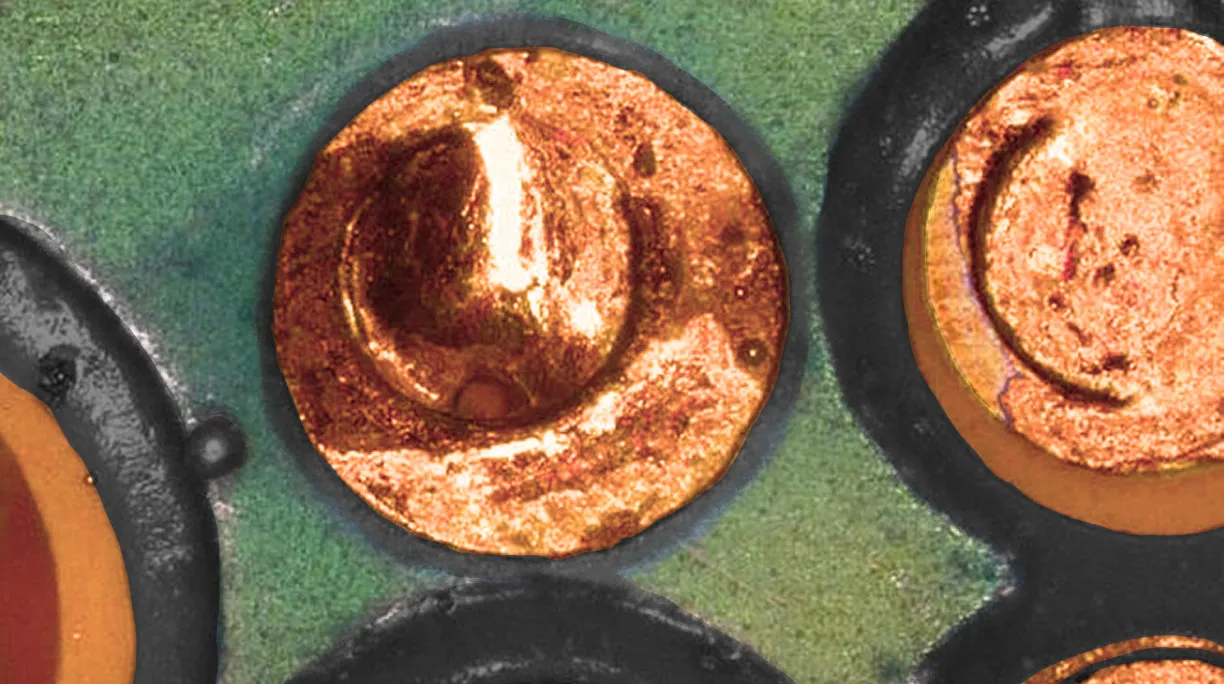
- Visual and Mechanical Inspection: Examine failed solder joints for signs of brittleness or cracking. Joints affected by black pad often show a flat, dark fracture surface at the nickel interface rather than a ductile failure within the solder itself.
- Thermal Cycling Tests: Subject assemblies to thermal cycling (e.g., -40°C to 125°C for 1000 cycles) to simulate real-world stress. Black pad-related failures often manifest as cracks after fewer than 500 cycles due to poor interfacial strength.
- X-Ray Inspection: Use X-ray imaging to check for voids or incomplete wetting in solder joints, especially under Ball Grid Array (BGA) components. Voids larger than 25% of the joint area can indicate black pad issues.
- Metallurgical Analysis: Perform cross-sectional analysis to study the intermetallic compound (IMC) layer at the solder-nickel interface. A thin or inconsistent IMC layer (less than 1 micrometer) often points to black pad as the cause of failure.
- Environmental Testing: Test assemblies in high-humidity or corrosive environments to assess long-term reliability. Black pad defects can accelerate joint degradation under such conditions, leading to failures in as little as 6-12 months.
Understanding the role of black pad in solder joint failures helps manufacturers pinpoint weaknesses in their processes and take corrective actions to improve overall reliability.
Case Study: Real-World Impact of Black Pad on PCB Reliability
To illustrate the real-world consequences of black pad, consider a scenario involving an automotive supplier producing engine control modules. After 12-18 months of vehicle deployment in regions with extreme temperature swings, field failures began to occur. Analysis revealed brittle fractures at BGA solder joints, with classic black pad symptoms visible under SEM inspection. The root cause was traced back to excessive phosphorus content in the nickel layer (above 11%) and poor bath chemistry control during ENIG plating.
By implementing stricter process controls, reducing phosphorus levels to 8%, and adopting regular SEM inspections, the supplier reduced failure rates by over 90%. This case highlights the importance of proactive measures in maintaining PCB surface finish reliability and preventing costly field failures.
Conclusion: Building Reliability Through Proactive Solutions
ENIG black pad is a challenging defect that can undermine the performance and reliability of PCBs, but it’s not an insurmountable problem. By understanding the ENIG black pad causes, implementing robust ENIG black pad prevention strategies, and using effective ENIG black pad detection methods, manufacturers can significantly reduce the risk of this issue. Additionally, thorough solder joint failure analysis ensures that any black pad-related issues are identified and addressed before they impact end users.
At ALLPCB, we are committed to helping manufacturers achieve the highest standards of PCB surface finish reliability. By following the practical steps outlined in this guide, you can protect your products from black pad defects and deliver reliable, high-quality PCBs to your customers. Focus on precision, consistency, and continuous improvement in your ENIG process, and you’ll build trust and reliability into every board you produce.