 ALLPCB


In the world of electronics, printed circuit boards (PCBs) are the backbone of every device, from smartphones to industrial machinery. However, even the smallest issues, like micro-cracks in PCB traces, can lead to catastrophic failures if left undetected. These tiny, often invisible cracks can disrupt signal integrity, cause intermittent faults, or even result in complete system breakdowns. So, how can you detect micro-cracks in PCB traces before they cause failure? The answer lies in advanced detection techniques, regular trace integrity testing, and a proactive approach to PCB reliability.
In this comprehensive guide, we’ll dive deep into the world of PCB micro-crack detection, explore methods for trace integrity testing, and discuss strategies for PCB failure analysis. We’ll also touch on hairline crack repair and share tips to improve overall PCB reliability. Whether you’re an engineer, designer, or manufacturer, this blog will equip you with the knowledge to protect your circuits from the silent killer of micro-cracks.
Understanding Micro-Cracks in PCB Traces: Why They Matter
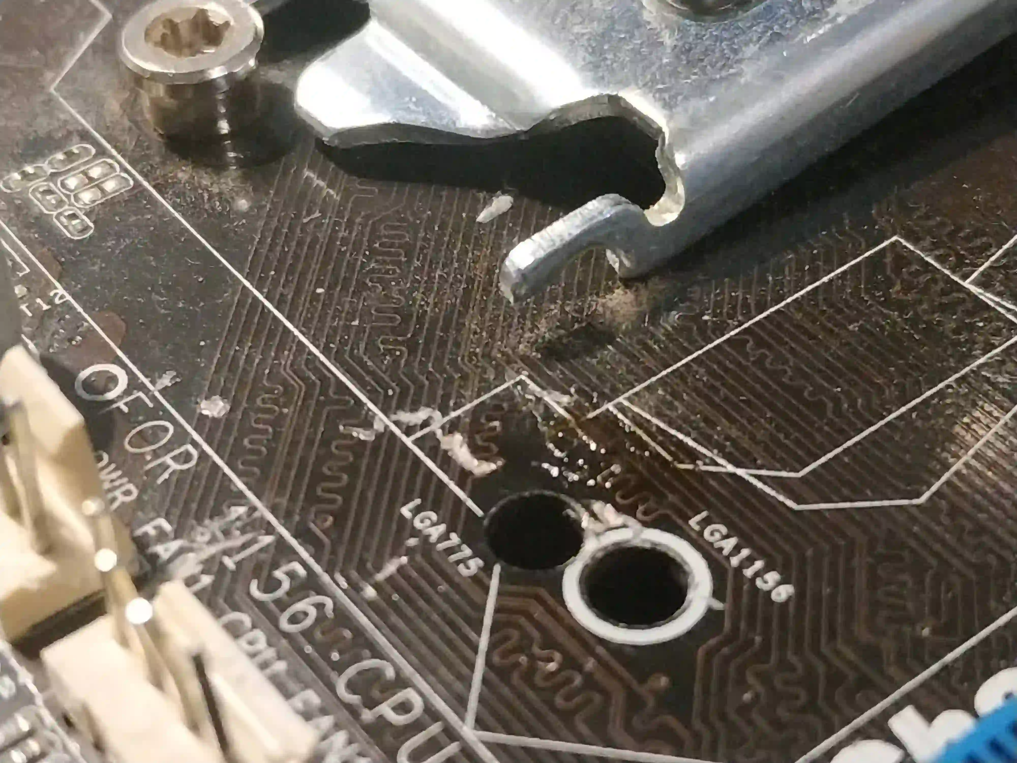
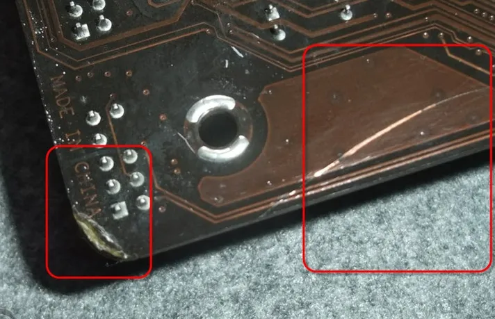
Micro-cracks are hairline fractures in the copper traces or solder joints of a PCB. Often measuring less than a few micrometers in width, these cracks are nearly impossible to spot with the naked eye. They can form due to various reasons, including thermal stress, mechanical strain, manufacturing defects, or environmental factors like humidity. While they may seem insignificant, micro-cracks can interrupt the flow of electrical signals, leading to issues like increased resistance, signal delays, or complete circuit failure.
For instance, a micro-crack in a high-speed signal trace could increase impedance beyond acceptable levels, say from a typical 50 ohms to 75 ohms or more, disrupting data transmission in a device. Over time, these small disruptions can escalate, causing intermittent errors or permanent damage. This is why early detection and prevention are critical for maintaining PCB reliability in any application, be it consumer electronics or aerospace systems.
Common Causes of Micro-Cracks in PCBs
Before we explore detection methods, it’s important to understand what causes micro-cracks in the first place. Identifying the root causes can help in both prevention and targeted testing. Here are some of the most common culprits:
- Thermal Stress: Repeated heating and cooling cycles during soldering or operation can cause the PCB material to expand and contract, leading to cracks in traces or vias. For example, a temperature swing from -40°C to 85°C can strain the board if not designed for such extremes.
- Mechanical Stress: Physical bending, vibration, or impact during assembly or use can fracture delicate traces. This is common in portable devices or automotive applications.
- Manufacturing Defects: Poor etching, over-etching, or improper lamination during production can weaken traces, making them prone to cracking.
- Environmental Factors: Exposure to moisture, chemicals, or extreme humidity can corrode or degrade copper traces over time, leading to hairline fractures.
By understanding these causes, engineers can design boards with better resilience and focus testing efforts on high-risk areas.
PCB Micro-Crack Detection: Techniques to Uncover Hidden Flaws
Detecting micro-cracks requires precision and the right tools, as these defects are often invisible to the naked eye. Below are some of the most effective methods for PCB micro-crack detection, each suited to different stages of production and testing.
1. Visual Inspection with Magnification
The simplest method for detecting micro-cracks is visual inspection under high magnification. Using a microscope with at least 10x to 50x magnification, technicians can spot hairline cracks in traces or solder joints. While this method is affordable and quick, it’s limited to surface-level defects and may miss internal cracks in multilayer boards.
2. Automated Optical Inspection (AOI)
AOI systems use high-resolution cameras and image processing software to scan PCBs for defects, including micro-cracks. These systems can detect anomalies as small as a few micrometers and are ideal for high-volume production. However, AOI is primarily effective for surface defects and may struggle with internal layers.
3. X-Ray Inspection
For multilayer PCBs, X-ray inspection is a powerful tool to detect internal micro-cracks. This non-destructive method uses X-ray imaging to reveal hidden fractures in traces, vias, and solder joints. It’s particularly useful for identifying cracks caused by thermal or mechanical stress in complex boards. While highly effective, X-ray systems can be expensive and require trained operators.
4. Microthermography
Microthermography, or thermal imaging, detects minute heat traces caused by electrical resistance in cracked areas. When a small current passes through a trace with a micro-crack, the resistance (often exceeding 10-20% of the normal value) generates localized heat, which can be captured by infrared cameras. This method is excellent for identifying functional issues but may not pinpoint the exact location of smaller cracks.
5. Dye Penetrant Testing
In dye penetrant testing, a fluorescent or colored dye is applied to the PCB surface. The dye seeps into any cracks or fractures, and under specific lighting (like UV light for fluorescent dyes), the cracks become visible. This method is effective for surface cracks but less practical for internal defects or assembled boards.
By combining these methods, manufacturers can ensure comprehensive detection of micro-cracks at various stages of PCB production and testing.
Trace Integrity Testing: Ensuring Signal Reliability
While detecting micro-cracks is crucial, testing the integrity of PCB traces ensures that signals are transmitted without loss or interference. Trace integrity testing focuses on electrical performance and can often reveal micro-cracks indirectly through anomalies in data. Here are key methods for trace integrity testing:
1. Continuity Testing
Continuity testing uses a multimeter or automated test equipment to check if a trace is intact. A break caused by a micro-crack will result in an open circuit, indicating failure. This method is simple and effective for detecting complete breaks but may miss partial cracks that still allow some current to pass.
2. In-Circuit Testing (ICT)
ICT uses a bed-of-nails fixture to contact test points on the PCB, measuring resistance, capacitance, and other parameters. For example, a trace with a micro-crack might show a resistance value far higher than the expected 0.1 ohms, indicating a potential issue. ICT is highly accurate for assembled boards but requires custom fixtures for each design.
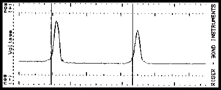
3. Time-Domain Reflectometry (TDR)
TDR is a sophisticated method that sends a high-speed electrical pulse through a trace and measures the reflected signal. A micro-crack will cause a change in impedance, visible as a spike or dip in the TDR waveform. This method is ideal for high-speed signal traces where even a small crack can disrupt performance, such as in traces designed for 5 GHz signals.
PCB Failure Analysis: Digging Deeper into Micro-Crack Issues
When micro-cracks are detected, or worse, when a PCB fails, conducting a thorough failure analysis is essential to understand the root cause. PCB failure analysis not only helps in addressing the immediate issue but also prevents future occurrences. Here’s how to approach it:
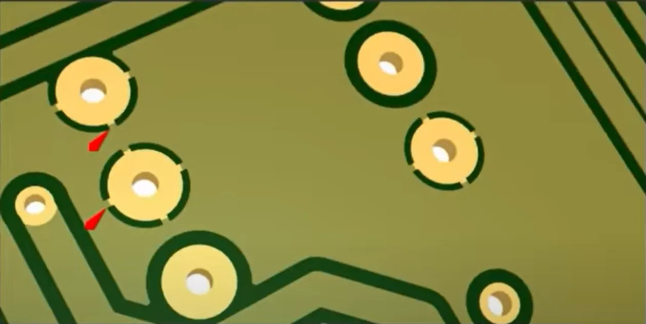
1. Visual and Microscopic Examination
Start with a detailed visual inspection under high magnification to identify the type and location of the crack. Is it a surface crack, a via failure, or an internal layer issue? This initial step guides further testing.
2. Electrical Testing
Use continuity, resistance, and signal integrity tests to confirm the impact of the crack. For instance, a cracked trace might show a resistance increase from 0.05 ohms to 1 ohm, directly affecting performance.
3. Cross-Sectional Analysis
For internal cracks, cut a cross-section of the PCB and examine it under a microscope. This destructive method reveals issues in multilayer boards, such as delamination or via cracks, that other methods might miss.
4. Environmental Testing
Simulate the conditions under which the PCB failed, such as temperature cycling between -55°C and 125°C or vibration testing at 10-55 Hz. This can help identify if thermal or mechanical stress caused the micro-crack.
By combining these techniques, engineers can pinpoint the cause of failure and implement design or process improvements.
Hairline Crack Repair: Can Micro-Cracks Be Fixed?
Repairing micro-cracks in PCB traces is often challenging, especially for hairline fractures in complex or multilayer boards. However, in some cases, repair is possible, particularly for surface-level cracks. Here are a few approaches:
- Soldering or Conductive Epoxy: For visible surface cracks, applying a small amount of solder or conductive epoxy can bridge the gap and restore continuity. However, this is a temporary fix and may not withstand long-term stress.
- Trace Rewiring: In cases where a trace is completely broken, a jumper wire can be soldered to bypass the damaged section. This method works for prototypes but isn’t practical for mass production.
- Board Replacement: For critical applications or internal cracks, replacing the PCB is often the safest option to ensure reliability.
While repair can be a quick fix, it’s always better to focus on prevention and early detection to avoid the need for such measures.
Improving PCB Reliability: Prevention Is Better Than Cure
The best way to deal with micro-cracks is to prevent them from occurring in the first place. Here are actionable tips to enhance PCB reliability:
- Design for Stress Tolerance: Use wider traces (e.g., 10 mils instead of 6 mils) in high-stress areas to reduce the risk of cracking. Incorporate thermal reliefs and proper via designs to handle temperature swings.
- Material Selection: Choose high-quality laminates and copper with good thermal and mechanical properties. For instance, FR-4 with a high Tg (glass transition temperature) of 170°C can better withstand heat stress.
- Controlled Manufacturing: Ensure strict quality control during etching, lamination, and soldering to avoid defects that lead to cracks.
- Environmental Protection: Apply conformal coatings or encapsulation to protect PCBs from moisture, dust, and chemical exposure.
- Regular Testing: Implement routine trace integrity testing and micro-crack detection during production and after assembly to catch issues early.
Conclusion: Stay Ahead of the Silent Killer
Micro-cracks in PCB traces are a silent killer that can undermine the reliability of even the most carefully designed electronics. By understanding their causes, employing advanced PCB micro-crack detection methods, and conducting regular trace integrity testing, you can catch these issues before they lead to failure. Additionally, thorough PCB failure analysis and proactive design improvements can significantly enhance PCB reliability, ensuring your products perform flawlessly in the field.
At ALLPCB, we are committed to helping you achieve the highest standards of quality and reliability in your PCB projects. From manufacturing to testing, our expertise and cutting-edge tools ensure that micro-cracks and other defects are identified and addressed early. Protect your designs from the silent killer of micro-cracks by integrating these strategies into your workflow today.


