ALLPCB


High aspect ratio vias represent a critical element in modern multilayer printed circuit boards. These structures enable dense interconnects in complex designs while supporting signal integrity and power distribution requirements. Designers encounter increasing demands for smaller form factors and higher layer counts, which push via geometries toward greater depth-to-diameter ratios. Effective management of these vias requires careful attention to both electrical performance and manufacturing feasibility.
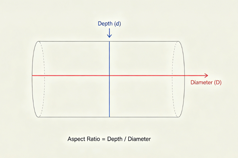
A via aspect ratio is calculated as the ratio of the board thickness or via depth to the drilled hole diameter. Ratios exceeding typical thresholds, such as those approaching or surpassing 8:1 for through-hole vias, classify as high aspect ratio. This parameter directly influences the feasibility of drilling and subsequent copper deposition processes. In advanced PCB design, high aspect ratio vias support greater routing density and shorter signal paths in high-speed applications.
Engineers must balance these benefits against potential impacts on yield and long-term reliability. Industry guidelines emphasize that exceeding recommended ratios increases the complexity of achieving uniform plating and structural integrity. Proper consideration during stack-up planning helps maintain overall board performance across thermal and mechanical stresses.
What Are High Aspect Ratio Vias and Why They Matter
A via aspect ratio is calculated as the ratio of the board thickness or via depth to the drilled hole diameter. Ratios exceeding typical thresholds, such as those approaching or surpassing 8:1 for through-hole vias, classify as high aspect ratio. This parameter directly influences the feasibility of drilling and subsequent copper deposition processes. In advanced PCB design, high aspect ratio vias support greater routing density and shorter signal paths in high-speed applications.
Engineers must balance these benefits against potential impacts on yield and long-term reliability. Industry guidelines emphasize that exceeding recommended ratios increases the complexity of achieving uniform plating and structural integrity. Proper consideration during stack-up planning helps maintain overall board performance across thermal and mechanical stresses.
Technical Principles of High Aspect Ratio Via Formation
Via formation begins with mechanical or laser drilling to create the hole through the dielectric and copper layers. As the aspect ratio increases, drill bits experience greater deflection and wear due to the extended penetration depth relative to diameter. This can result in rougher hole walls or positional inaccuracies that affect subsequent steps.
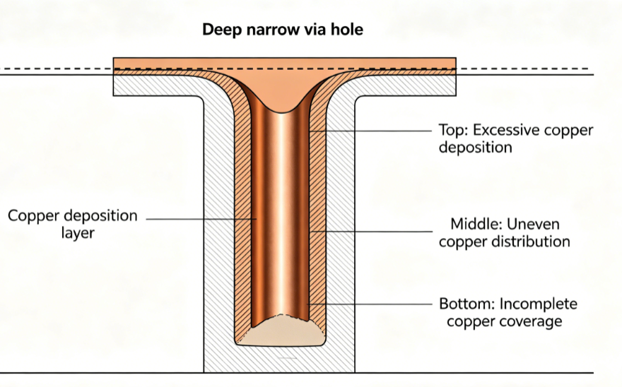
Plating follows drilling, where electroplating solutions must penetrate the narrow channel to deposit copper uniformly along the walls. Higher ratios hinder solution flow and mass transport, often leading to thinner deposits in the middle sections compared to the ends. Such nonuniformity raises risks of voids or weak points under thermal cycling.
Standards such as those outlined in IPC-6012 address qualification requirements for plated through-holes to ensure minimum copper thickness and coverage. Designers evaluate these mechanisms early to predict manufacturability.
PCB Manufacturing Challenges with High Aspect Ratio Vias
Drilling high aspect ratio vias introduces several process constraints. Smaller diameter tools required for elevated ratios consume faster and demand precise control of feed rates and spindle speeds to prevent breakage. Hole wall quality suffers when debris removal becomes inefficient in deeper cavities, potentially compromising adhesion for plating.
Plating uniformity presents another significant hurdle. Capillary action and throwing power of the electrolyte diminish with increasing depth, making it harder to achieve consistent wall thickness throughout the via. This challenge intensifies in thicker boards or those with multiple lamination cycles.
Via drilling techniques must adapt accordingly, often incorporating optimized parameters or sequential processes to maintain hole integrity. These factors collectively contribute to higher scrap rates if not addressed through design adjustments.
Best Practices for High Aspect Ratio Via Design Rules
Designers begin by targeting aspect ratios within established practical limits for through-hole vias, commonly up to 10:1 depending on board thickness and fabricator capabilities. Selecting larger drill diameters where possible reduces the ratio while preserving necessary connectivity. Early collaboration on stack-up configuration helps distribute vias to avoid localized concentrations that exacerbate processing difficulties.
For microvias, guidelines recommend lower ratios, typically not exceeding 1:1, to facilitate reliable laser drilling and filling. Incorporating via filling or capping can enhance structural support in demanding applications. Simulation of thermal and mechanical stresses during the design phase provides additional validation of via performance.
Adherence to design guidelines in IPC-2221 supports consistent annular ring dimensions and land sizing that complement via geometry choices. Regular design rule checks tailored to high aspect ratio scenarios minimize iterations during fabrication.
Practical Solutions and Advanced Techniques
Advanced via drilling techniques include controlled-depth drilling for blind structures and process optimizations such as peck drilling cycles to improve chip evacuation. These approaches help sustain hole quality even as ratios increase. Plating process adjustments, including modified electrolyte formulations or current density profiles, improve throwing power for deeper vias.
Back-drilling or controlled-depth techniques can remove unused via stubs in high-speed designs, reducing signal integrity concerns associated with longer paths. Sequential lamination builds complex structures incrementally, allowing intermediate plating steps that ease overall aspect ratio demands.
Verification through cross-section analysis and electrical testing confirms that design intent translates into reliable hardware. These solutions integrate into standard workflows when applied systematically.
Conclusion
High aspect ratio vias enable advanced PCB designs but require deliberate engineering attention to drilling, plating, and reliability factors. Structured application of design rules and manufacturing-aware choices supports successful outcomes. Ongoing reference to established standards ensures consistency across projects.
FAQs
Q1: What defines high aspect ratio via design rules in PCB layouts?
A1: High aspect ratio via design rules specify limits on the depth-to-diameter ratio to ensure reliable drilling and plating. Typical guidelines recommend keeping through-hole via ratios at or below 10:1 for standard boards, with adjustments based on thickness and process capabilities. Following these rules helps maintain plating uniformity and structural integrity in multilayer constructions.
Q2: How do PCB manufacturing challenges affect high aspect ratio vias?
A2: PCB manufacturing challenges with high aspect ratio vias include drill deflection, hole wall roughness, and difficulties achieving uniform copper plating throughout the depth. These issues can lead to voids or reduced reliability if the ratio exceeds practical limits. Early design adjustments mitigate many of these concerns during fabrication.
Q3: What via drilling techniques support advanced PCB design with elevated aspect ratios?
A3: Via drilling techniques for advanced PCB design incorporate optimized speeds, feeds, and peck cycles to manage deeper holes without compromising quality. Laser drilling offers alternatives for smaller features with lower aspect ratios. Selection of the appropriate method depends on the target geometry and board stack-up.
Q4: Why is aspect ratio important for via reliability in electrical engineers' projects?
A4: Aspect ratio influences copper deposition quality and thermal-mechanical performance of vias. Higher ratios increase the potential for plating inconsistencies that affect conductivity and long-term durability under operational stresses. Careful ratio management supports consistent results in demanding applications.
References
IPC-6012E — Qualification and Performance Specification for Rigid Printed Boards. IPC, 2017
IPC-T-50M — Terms and Definitions for Interconnecting and Packaging Electronic Circuits. IPC, 2015
IPC-2221B — Generic Standard on Printed Board Design. IPC, 2012