ALLPCB


Introduction
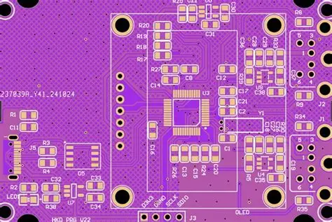
High speed digital designs often encounter signal integrity challenges when signals travel through printed circuit boards. Vias, which connect different layers, can introduce unwanted electrical effects that degrade performance at elevated frequencies. Backdrilling addresses one specific aspect of these challenges by targeting the unused portion of the via. This technique has become relevant for engineers working with faster data rates and more complex multilayer boards. Understanding its fundamentals helps designers make informed decisions during layout and fabrication planning. The process aligns with established practices in rigid board qualification under IPC 6012E.
What Is Backdrilling and Why It Matters
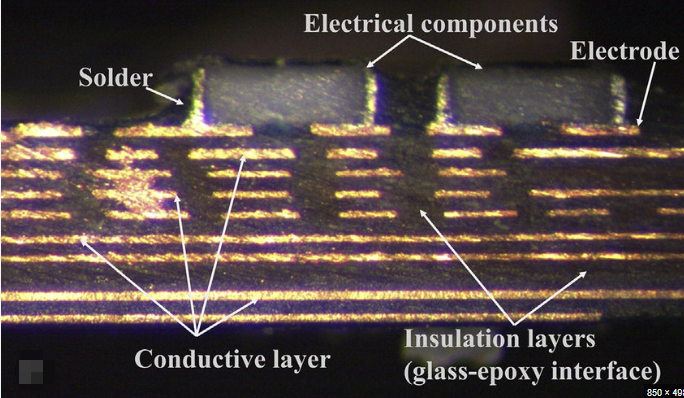
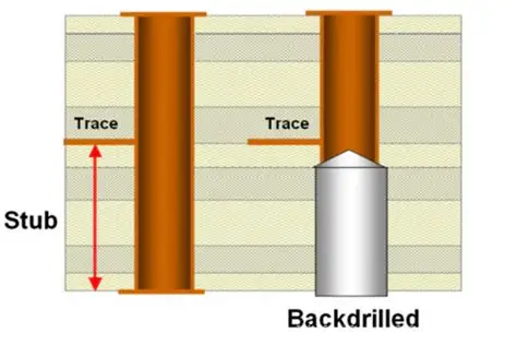
Backdrilling removes the conductive barrel segment of a plated through hole that extends beyond the intended signal path. This unused segment is commonly called a via stub. In a standard through hole via, the barrel runs from one outer layer to the opposite outer layer even when the signal only needs to connect two inner layers. The resulting stub acts as an open transmission line stub that can cause reflections. These reflections distort the signal waveform and reduce the effective bandwidth of the interconnect. For hobbyists exploring high speed interfaces such as PCIe or high speed serial links, recognizing this effect early in the design process supports better board performance. The relevance grows as clock frequencies increase and edge rates shorten, making even small discontinuities noticeable. Industry standards such as IPC 2221 provide guidance on via design considerations that complement backdrilling decisions.
Technical Principles of Via Stub Removal
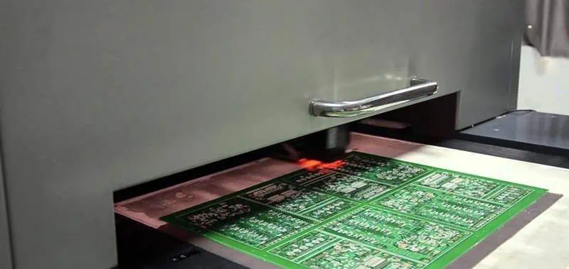
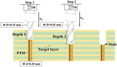
A via forms when a drill creates a hole through the board stack up followed by copper plating of the hole walls. When the signal route changes layers at an inner layer, the plating below that layer remains electrically connected but carries no intentional current. This creates a resonant structure whose length corresponds to a quarter wavelength at certain frequencies. The resonance produces impedance discontinuities that reflect portions of the incident signal energy back toward the source. Backdrilling uses a controlled depth drill from the opposite side of the board to remove most of the unused plating without damaging the functional via segment. The remaining stub length is typically reduced to a few mils, which shifts the resonant frequency well above the operating bandwidth. Proper control of drill depth and alignment ensures the functional connection stays intact while minimizing the stub. These mechanisms follow logical cause and effect relationships that engineers can model using transmission line theory during simulation.
Practical Solutions and Best Practices
Designers begin by identifying which vias carry high speed signals and calculating the maximum acceptable stub length based on the target data rate. Layer stack up planning plays a central role because backdrilling is most effective when the signal transition occurs several layers away from the board surface. During layout, placing the via transition closer to the surface reduces the initial stub length and may eliminate the need for backdrilling in some cases. When backdrilling is required, communication with the fabricator includes specifying the backdrill depth, diameter, and tolerance to match the board thickness and copper weight. Fabrication notes should reference the relevant sections of IPC 6012E to ensure the finished board meets acceptance criteria for via integrity after the secondary drilling operation. Post fabrication inspection often includes cross section analysis to verify stub removal depth and confirm that the remaining barrel maintains adequate plating thickness. Hobbyists working on prototype boards can request backdrilling on selected vias while keeping other vias as standard through holes to balance cost and performance.
Conclusion
Backdrilling provides a targeted method to reduce via stub effects that otherwise limit signal integrity in high speed PCB designs. By understanding the formation of stubs and the controlled removal process, engineers can decide when the technique adds value without unnecessary complexity. Structured planning around layer transitions, fabrication tolerances, and verification steps leads to consistent results across prototype and production boards. The approach integrates naturally with existing design workflows and aligns with qualification requirements outlined in applicable IPC standards. Hobbyists who incorporate these considerations early gain greater confidence in achieving reliable performance at elevated operating frequencies.
FAQs
Q1: What is backdrilling in PCB manufacturing?
A1: Backdrilling is a secondary drilling operation that removes the unused portion of a plated through hole barrel after the primary via formation. The process shortens the via stub that would otherwise remain connected to the signal path. Reduced stub length minimizes reflections and improves signal quality for high speed circuits. The technique applies selectively to vias carrying critical signals rather than every via on the board.
Q2: How does via stub removal improve signal integrity?
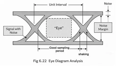
A2: A via stub creates an impedance discontinuity that reflects portions of the propagating signal. Removing most of the stub shortens the resonant length and moves unwanted resonances outside the operating frequency range. The result appears as cleaner waveforms and wider eye openings in high speed serial links. Designers evaluate the benefit through simulation before committing to the backdrilling step.
Q3: When should a beginner consider backdrilling for a project?
A3: Beginners should evaluate backdrilling when the design includes data rates above a few gigabits per second and the layer transition creates a stub longer than approximately ten mils. Early stack up review helps identify candidate vias. Collaboration with the board fabricator confirms feasibility and cost impact before layout finalization.
Q4: What standards guide backdrilling implementation?
A4: IPC 6012E outlines qualification and performance requirements for rigid printed boards including via structures after secondary operations. IPC 2221 supplies design recommendations that inform via placement decisions related to stub management. These documents help ensure the finished board meets acceptance criteria without introducing new defects during backdrilling.
References
IPC-6012E — Qualification and Performance Specification for Rigid Printed Boards. IPC, 2017
IPC-2221 — Generic Standard on Printed Board Design. IPC, 2012
IPC-A-600K — Acceptability of Printed Boards. IPC, 2020