ALLPCB


Why Signal Integrity Matters in Transportation PCBs
Transportation environments expose PCBs to vibration, temperature swings, and electromagnetic interference. These factors can degrade high-speed signals if signal integrity is not managed from the start. Automotive radar systems, for example, depend on clean high-frequency transmission to detect objects accurately. Impedance control transportation PCB practices help maintain consistent signal paths across boards. Without attention to these details, reflections and noise can compromise system accuracy and response times.
Signal integrity analysis forms the foundation for evaluating how signals behave on a board. Engineers simulate propagation delays, rise times, and return paths to identify potential issues early. In transportation applications, even small distortions may lead to false readings or delayed commands. Structured analysis supports compliance with performance expectations in safety-related systems. This approach reduces the need for costly revisions after prototypes are built.
Technical Principles of Signal Integrity
High-speed signals travel along PCB traces as electromagnetic waves. When trace impedance varies, part of the signal reflects back toward the source. These reflections combine with the original waveform and create distortion. Differential signaling helps cancel common-mode noise, yet it requires precise length matching and spacing. Ground planes provide low-impedance return paths that minimize loop inductance.
Crosstalk occurs when energy from one trace couples into an adjacent trace. The effect grows with faster edge rates and closer trace spacing. Engineers calculate coupling coefficients and adjust routing to keep crosstalk within acceptable limits. Power distribution networks must also deliver stable voltage at high frequencies. Decoupling capacitors placed near integrated circuits supply transient current and reduce voltage droop.
Practical Solutions and Best Practices
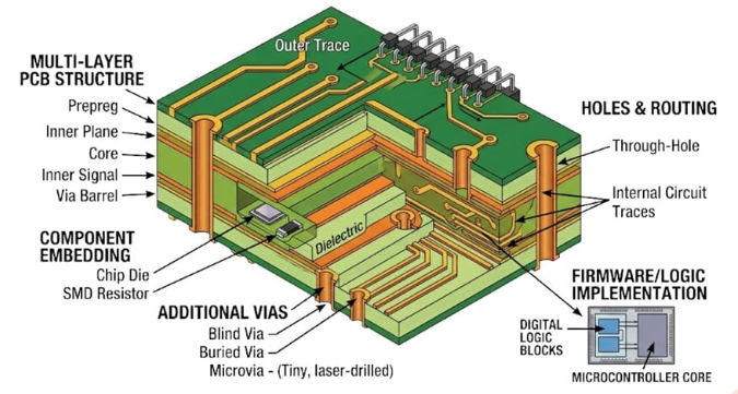
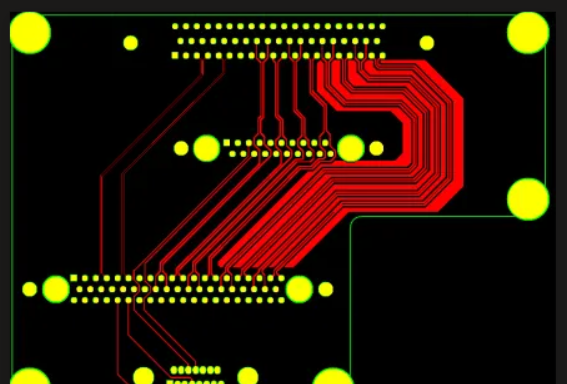
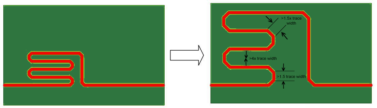
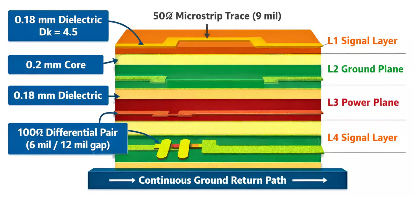
Designers begin with stack-up planning to achieve target impedance values. Controlled dielectric thickness and copper weight allow calculation of trace width for single-ended and differential pairs. PCB trace routing rules include maintaining consistent spacing, avoiding sharp bends, and using smooth curves where turns are necessary. Length matching within pairs ensures signals arrive simultaneously at the receiver.
Via placement requires care because each via introduces inductance and potential impedance discontinuity. Back-drilling or blind vias reduce stub effects in very high-speed designs. Ground stitching vias connect reference planes and provide short return paths. Shielding techniques, such as ground pours around sensitive traces, further limit radiated emissions.
Minimizing EMI in transportation PCBs involves both layout and material choices. Continuous ground planes beneath signal layers contain fields and reduce radiation. Proper partitioning separates analog, digital, and power sections. Filtering at connectors and careful clock routing prevent emissions from reaching external antennas or other subsystems.
Additional Considerations for Transportation Applications
Transportation PCBs often operate across wide temperature ranges. Material selection must account for coefficient of thermal expansion to prevent stress on copper traces and vias. High-speed digital PCB design automotive radar modules requires particular attention to phase stability because small timing errors affect distance measurement accuracy. Thermal management features, such as thermal vias and heat-spreading planes, keep components within operating limits during continuous use.
Testing protocols verify that boards meet signal integrity targets before deployment. Time-domain reflectometry measures impedance along traces, while vector network analyzers characterize frequency response. These measurements confirm that design simulations align with physical hardware performance.
Conclusion
Effective high-speed digital PCB design in transportation depends on consistent attention to signal integrity throughout the development process. Impedance control, careful trace routing, and EMI mitigation work together to deliver reliable data transmission. Engineers who apply structured analysis and follow established layout practices reduce the risk of performance issues in the field. These methods support the demanding requirements of automotive radar, rail signaling, and avionics systems.
FAQs
Q1: What role does impedance control play in high-speed PCB design for automotive radar?
A1: Impedance control ensures that transmission lines match the characteristic impedance of connected components. This matching minimizes reflections and preserves signal shape at high frequencies. In automotive radar applications, controlled impedance supports accurate timing and amplitude of transmitted and received pulses. Designers calculate trace geometry based on dielectric properties and copper thickness to achieve target values across the operating temperature range.
Q2: How does signal integrity analysis improve PCB performance in transportation systems?
A2: Signal integrity analysis identifies reflections, crosstalk, and timing skew before hardware fabrication. Engineers use simulation tools to model trace behavior and adjust routing accordingly. The process helps maintain data integrity in environments with vibration and electromagnetic noise. Results guide decisions on layer stack-up, via placement, and termination strategies that enhance overall system reliability.
Q3: What PCB trace routing rules help minimize EMI in transportation PCBs?
A3: Routing rules include maintaining adequate spacing between high-speed traces, using ground planes for return paths, and avoiding unnecessary vias. Differential pairs should be routed with consistent separation and length matching. Clock lines benefit from shielding or guard traces to contain fields. These practices reduce radiated emissions and improve immunity to external interference common in transportation settings.
Q4: Why is minimizing EMI important for high-speed digital designs in transportation?
A4: Electromagnetic interference can corrupt data or cause false triggers in safety-critical functions. Transportation platforms contain multiple electronic systems operating simultaneously, increasing the chance of coupling between circuits. Careful layout, grounding, and filtering limit emissions and susceptibility. Compliance with relevant electromagnetic compatibility expectations supports safe and dependable operation across vehicle fleets.
References
IPC-6012E — Qualification and Performance Specification for Rigid Printed Boards. IPC, 2017
IEC 61000 series — Electromagnetic Compatibility. IEC
JEDEC J-STD-020E — Moisture/Reflow Sensitivity Classification. JEDEC, 2014