 ALLPCB


Introduction
Heavy copper PCBs represent a critical advancement in printed circuit board technology, particularly for applications demanding superior current handling and heat dissipation. These boards feature copper layers significantly thicker than standard 1 oz per square foot foils, enabling them to support high power applications where conventional designs fail under thermal or electrical stress. Engineers designing for industrial environments often turn to heavy copper PCB solutions to ensure reliability in rugged PCB design scenarios, such as power inverters or motor controls. The shift to thicker copper, measured in mils, addresses limitations in trace width and layer count while optimizing overall board performance. As power densities increase in modern electronics, understanding when to specify extreme copper thickness becomes essential for thermal management PCB strategies. This article explores the principles, applications, and best practices for implementing heavy copper in demanding industrial PCB design.
What Are Heavy Copper PCBs and Why Do They Matter?
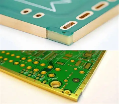
Heavy copper PCBs are defined by copper weights exceeding 3 oz per square foot, translating to thicknesses greater than approximately 4 mils per layer after processing. Standard PCBs typically use 1 oz copper, which equates to about 1.37 mils, sufficient for low-power signal routing but inadequate for high-current paths. In contrast, heavy copper layers range from 3 oz (around 4.11 mils) to 10 oz or more (over 13 mils), providing enhanced durability and efficiency. This thickness is crucial in high power applications like welding equipment or electric vehicle power modules, where sustained currents generate substantial heat.
The relevance of heavy copper PCBs stems from their ability to carry higher currents without excessive temperature rise, directly impacting system reliability. Thicker copper reduces voltage drop and improves mechanical strength, making them ideal for rugged PCB design in vibration-prone industrial settings. Thermal management PCB performance improves as copper's high thermal conductivity spreads heat laterally across the board. For electric engineers, selecting heavy copper prevents hotspots and extends component lifespan in continuous operation.
- Copper Weight: 1 oz/ft2 - Nominal Thickness: 1.37 mils - Typical Applications: Signal layers
- Copper Weight: 2 oz/ft2 - Nominal Thickness: 2.74 mils - Typical Applications: Moderate power
- Copper Weight: 3 oz/ft2 - Nominal Thickness: 4.11 mils - Typical Applications: Heavy copper start
- Copper Weight: 5 oz/ft2 - Nominal Thickness: 6.85 mils - Typical Applications: High power
- Copper Weight: 10 oz/ft2 - Nominal Thickness: 13.7 mils - Typical Applications: Extreme thickness
This list illustrates the progression, guiding initial specifications.
Technical Principles of Heavy Copper Thickness
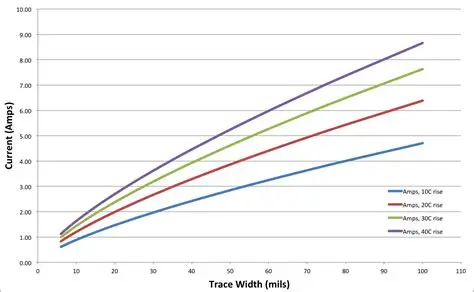
The core principle driving heavy copper PCB use is increased current-carrying capacity, governed by factors like trace cross-section and allowable temperature rise. According to IPC-2221, current capacity scales with copper thickness and width, allowing narrower traces for the same amperage compared to standard foils. For instance, a 100-mil wide trace at 3 oz copper handles significantly more current than at 1 oz, reducing board real estate needs. This is vital in compact high power applications where space constraints limit layer stacking.
Thermal management PCB efficacy relies on copper's thermal conductivity of about 400 W/mK, far superior to dielectric materials. Thicker layers act as heat spreaders, lowering via temperatures and preventing delamination under thermal cycling. However, extreme thicknesses introduce challenges like differential etching rates, where inner trace edges etch slower, potentially causing undercuts. Engineers must balance these effects during layout to maintain impedance control and signal integrity in mixed-signal designs.
Mechanical properties also shift with thickness; heavier copper enhances rigidity but increases warpage risk during lamination due to CTE mismatches. IPC-6012 specifies qualification tests for such boards, ensuring they withstand flexure and thermal shock. In industrial PCB design, this robustness supports operation in harsh environments with high vibration or humidity.
When to Specify Extreme Copper Thickness in Mils
Extreme copper thickness, typically beyond 6 mils (roughly 4 oz or more), is warranted when standard heavy copper falls short in high power applications. Consider scenarios like aerospace power supplies or rail traction systems, where currents exceed 50 A per trace continuously. Here, 10-mil layers (about 7 oz) minimize I^2R losses and support direct heatsink attachment without intermediate busbars. Thermal simulations often reveal that such thicknesses keep junction temperatures under 125°C even at peak loads.
Rugged PCB design benefits from extreme copper in mining equipment or renewable energy inverters, where mechanical stress combines with thermal cycling. Thinner foils risk cracking at vias under vibration, while thick copper provides strain relief. However, use extreme thickness judiciously; boards over 12 mils demand specialized plating to fill vias adequately, avoiding voids that compromise interlayer connections.
Thresholds for adoption include power levels above 1 kW per square inch or environments exceeding 85°C ambient. If finite element analysis shows standard 3-oz traces exceeding 30°C rise, upgrade to 5 mils or more. Industrial PCB design teams should prototype with varying thicknesses to validate against reliability targets.
Best Practices for Rugged PCB Design with Heavy Copper
Start with stack-up optimization, pairing thick copper with high-Tg laminates to mitigate warpage in thermal management PCB layouts. Sequential lamination builds outer heavy layers separately, adhering to IPC guidelines for controlled expansion. Trace geometries require wider spaces; for 5-oz copper, minimum trace/space often exceeds 10 mils to prevent shorts during etching.
Via design is critical: use filled or plated-through holes with copper caps to handle current without necking. IPC-A-600 defines acceptability criteria for plating uniformity in heavy copper features. Incorporate thermal vias under high-power components, arrayed to channel heat to inner planes.
Manufacturing tolerances tighten with thickness; specify ±10% per IPC-4562, but verify post-etch. For rugged applications, apply conformal coatings over exposed copper to resist corrosion. Simulate thermomechanical stress early to predict bow and twist limits.
In high power applications, integrate copper pours for ground planes, enhancing EMI shielding alongside thermal paths. Test boards per IPC-TM-650 methods for current endurance and thermal cycling.
Applications in Demanding High Power Environments
In electric vehicle inverters, heavy copper PCBs manage hundreds of amps from battery packs, with 8-mil outer layers dissipating MOSFET heat effectively. Industrial motor drives use 6-mil thicknesses for frequency converters, enduring 10g vibrations without trace lifts. Welding machines rely on 10-oz planes for transformer primaries, where extreme thickness prevents meltdown during arc strikes.
Renewable energy systems, like solar string inverters, benefit from thermal management PCB features with 5-mil copper balancing cost and performance. Defense radar power amps specify rugged PCB design with filled vias in 12-mil layers for pulsed high currents. These examples highlight when extreme copper elevates reliability over standard alternatives.
Conclusion
Heavy copper PCBs, especially with extreme thicknesses beyond 6 mils, unlock performance in high power applications requiring robust thermal management and rugged PCB design. By leveraging principles from IPC standards, engineers can specify thicknesses that match current demands while mitigating risks like warpage and etching defects. Practical implementation through optimized stack-ups and testing ensures industrial PCB design success. Prioritize simulations and prototypes to determine exact needs, balancing benefits against fabrication complexity. Ultimately, heavy copper enables compact, reliable systems in the most demanding environments.
FAQs
Q1: What defines a heavy copper PCB, and how does thickness in mils impact high power applications?
A1: Heavy copper PCBs feature layers over 3 oz per square foot, or more than 4 mils thick, ideal for high power applications. Thicker copper, like 6-13 mils, boosts current capacity and thermal dissipation, reducing trace widths and board size. This supports sustained high amps without excessive heat buildup. Design per IPC-2221 for optimal performance.
Q2: When should electric engineers choose extreme copper thickness over standard heavy copper for thermal management PCB?
A2: Opt for extreme thickness (over 10 mils) in thermal management PCB for apps exceeding 50 A continuous or 100°C rises. It's essential for rugged PCB design in EVs or industrial drives where standard 4 mils insufficiently spreads heat. Verify via simulations showing hotspots. This prevents failures in high power applications.
Q3: What are key best practices for industrial PCB design using heavy copper?
A3: Follow wider trace/space rules, filled vias, and high-Tg materials for industrial PCB design with heavy copper. Use differential etching and sequential lamination to control warpage. Test per IPC-6012 for qualification. These ensure reliability in rugged environments with vibration and heat.
Q4: How does heavy copper improve rugged PCB design in demanding applications?
A4: Heavy copper enhances mechanical strength and current handling in rugged PCB design, resisting thermal cycling and vibration. Thicker layers reduce impedance and aid heat spreading for high power applications. It's suited for welding or aerospace where durability trumps cost.
References
IPC-6012E - Qualification and Performance Specification for Rigid Printed Boards. IPC, 2017
IPC-2221B - Generic Standard on Printed Board Design. IPC, 2012
IPC-A-600K - Acceptability of Printed Boards. IPC, 2020


