 ALLPCB


Introduction
Laser drilling has opened up exciting possibilities for electronic hobbyists looking to push the boundaries of consumer electronics mods. Imagine taking apart a gadget, exposing its printed circuit board, and using a precise laser beam to create custom vias, slots, or apertures that enable new functionalities like adding sensor ports or rerouting signals. This advanced DIY technique goes beyond basic soldering, allowing for micro-scale modifications that mechanical tools simply cannot match in precision. For those passionate about electronics mods, laser drilling hacking represents a gateway to highly customized projects, from enhancing audio devices to prototyping embedded upgrades. However, success demands a solid understanding of laser physics, material interactions, and safety protocols to avoid damaging delicate boards. In this guide, we explore the principles, setups, and best practices to help you master laser cutting electronics in your workshop.
What Is Laser Drilling Hacking and Why It Matters for Electronics Mods
Laser drilling hacking involves using focused laser energy to ablate material from existing PCBs in consumer devices, creating precise features for advanced DIY modifications. Unlike traditional mechanical drilling, which risks cracking thin boards or wandering off-target, lasers deliver non-contact ablation with tolerances down to microns, ideal for densely packed circuits. This technique matters because modern consumer electronics feature multilayer boards with fine-pitch components, where even minor mods require sub-millimeter accuracy to maintain signal integrity. Hobbyists use it for tasks like drilling blind vias to stack components, cutting custom slots for flex cables, or exposing hidden test points without delaminating layers. As devices grow smaller and more integrated, laser drilling enables electronics mods that were once factory-only, empowering creators to extend hardware life or add bespoke features. The relevance spikes in high-density interconnect scenarios, where standards like IPC-6012E specify performance for rigid printed boards including laser-formed features.
Technical Principles of Laser Drilling on Consumer PCBs
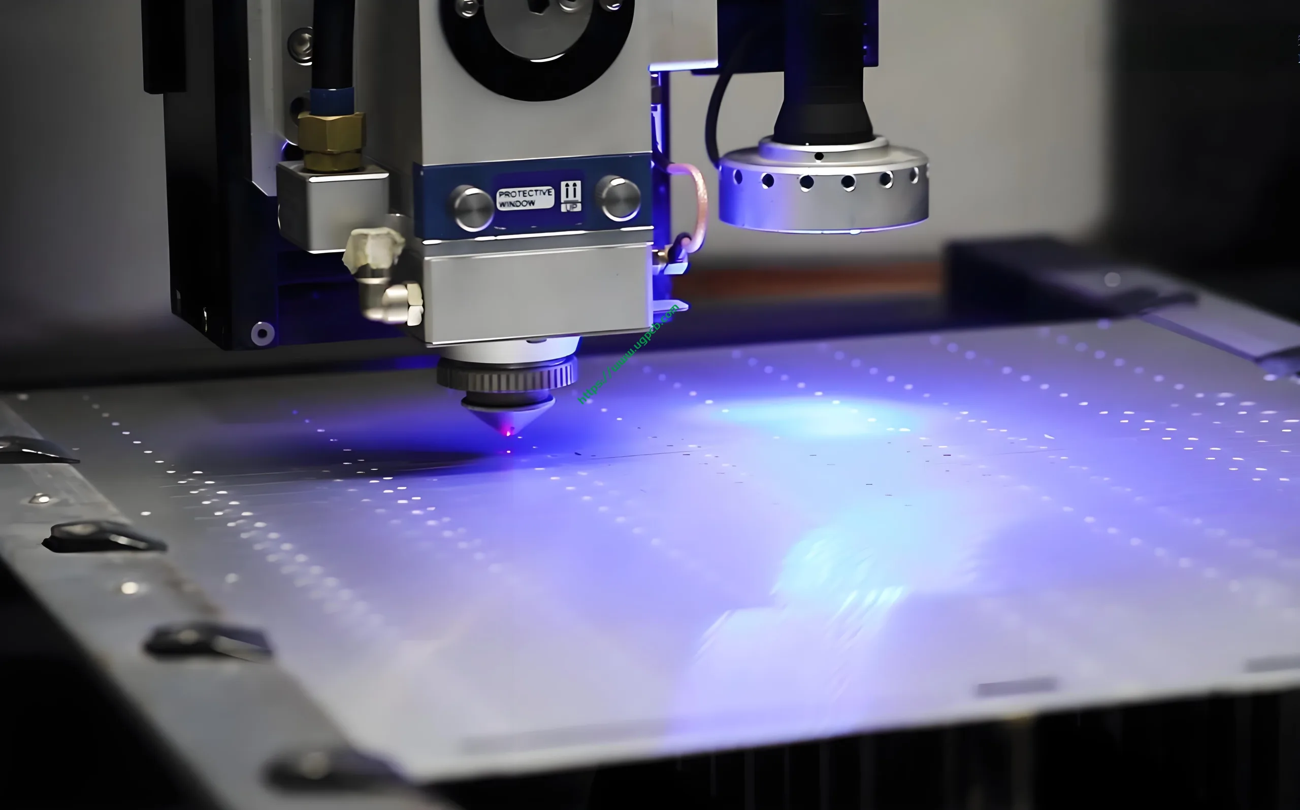
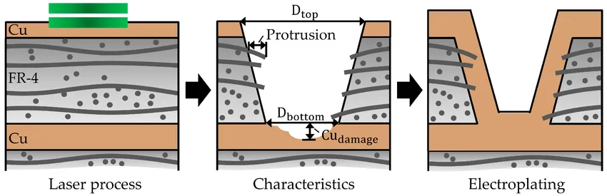
At its core, laser drilling relies on photothermal or photochemical ablation, where a high-energy beam vaporizes material layer by layer without physical contact. For FR4 substrates common in consumer electronics, CO2 lasers at 10.6 micrometers wavelength excel at cutting through epoxy resin and glass fibers, while UV or fiber lasers handle finer blind vias by breaking molecular bonds. The process starts with beam focusing via lenses to a spot size of 20-50 microns, pulsing at kilohertz rates to control heat-affected zones and prevent charring. Key parameters include power density, typically 10-100 J/cm2, pulse duration under 100 nanoseconds, and scan speed to balance removal rate with thermal damage. Material absorption varies: copper reflects infrared light poorly, requiring multiple passes or preprocessing, whereas dielectrics like resin absorb efficiently for clean holes. Adhering to aspect ratios under 1:1, as guided by design standards, ensures reliable plating if vias need conductivity post-mod.
Consumer PCBs present unique challenges due to their heterogeneous stackup of copper, resin, and solder mask. Lasers must navigate solder mask first, which ablates cleanly at lower energies, then penetrate dielectric without resin smear that could short circuits. Overheating risks carbonization, reducing insulation resistance, so assist gases like nitrogen help eject debris and cool the site. For multilayer boards, sequential drilling from both sides aligns stacked vias precisely, mimicking high-density interconnect methods. Understanding fluence thresholds—energy per unit area—prevents microcracks, aligning with IPC acceptability criteria for hole quality. These principles transform laser drilling into a repeatable tool for electronics mods, far surpassing handheld drills in precision.
Essential Safety and Workspace Setup for Advanced DIY Laser Drilling
Safety forms the foundation of any laser drilling project, especially when modding live-harvested PCBs from consumer devices. Always wear laser-specific goggles matching the wavelength—CO2 requires 10.6μm blockers—along with gloves and respirators to counter fumes from ablating epoxy or plastics. Enclose the laser in a ventilated cabinet with exhaust rated for particulates, directing smoke away from the workspace to prevent buildup of flammable residues. Keep a Class D fire extinguisher handy, as molten copper or ignited resin poses ignition risks during prolonged runs. Never operate unattended, and perform test fires on scrap material to calibrate without risking the target board. Regular maintenance, like cleaning optics and alignment checks, ensures consistent beams and avoids stray reflections.
Setting up your station starts with a stable, vibration-free table supporting the laser head over a fixturing jig for the PCB. Use sacrificial backers like acrylic sheets to capture ejecta and protect the laser bed. Software like EZCAD or LightBurn imports Gerber-like paths for drilling patterns, allowing G-code generation from mods designed in free tools. Fixture the disassembled board with vacuum hold-downs or tape to prevent movement, critical for sub-100-micron features. Integrate a camera for live preview, enabling real-time adjustments during electronics mods. This setup not only boosts accuracy but complies with general lab safety aligning with ISO 11553 for laser machinery.
Advanced Techniques for Laser Drilling in Electronics Mods
One powerful technique is microvia formation for stacking SMD components on existing pads, starting with low-power passes to remove solder mask, then ramping energy for dielectric penetration. For rerouting signals in consumer gadgets, laser-cut narrow slots isolate traces, followed by jumper wires soldered across. Precision drilling for headers involves patterning arrays at 0.5mm pitch, centering on ground planes to minimize inductance—test with continuity probes post-ablation. In multilayer mods, blind vias connect inner layers; use pulsed UV lasers for 50-micron entrances tapering to 75 microns, plating with conductive ink for DIY interconnects. Troubleshooting charring? Reduce pulse overlap and introduce air assist to clear vaporized material mid-process.
Another advanced method targets flex-rigid hybrids in wearables: laser ablation creates fanout apertures for daughterboard attachment, preserving flex integrity. For audio hacks, drill phased-array holes for custom microphones, spacing per acoustic design. Always verify hole geometry with optical profilometry or microscope, ensuring wall roughness under 5 microns per IPC-A-600 guidelines for acceptability. Combine with depaneling—outline cuts at vector mode—to liberate modded sections cleanly. These techniques elevate laser drilling hacking, turning stock PCBs into feature-rich prototypes.
Case studies from hobbyist forums highlight successes: one modder drilled JTAG access on a compact controller board, enabling firmware tweaks without full redesign. Another cut ventilation slots in a power module, improving thermal performance while maintaining EMI shielding. Common pitfalls include misalignment from thermal expansion—mitigate with fiducials—and debris shorts, cleared via ultrasonic baths. Iterate designs in simulation first, predicting ablation depth from material datasheets.
Best Practices and Troubleshooting for Reliable Results
Optimize parameters iteratively: begin with 20% power on scrap FR4, increasing until breakthrough without haloing. Maintain focus height within 0.1mm tolerance using autofocus probes. Post-drill, inspect for taper—ideal 1-2 degrees—and desmear with plasma or chemical permanganate for plating readiness. For production-like quality in DIY, batch-process multiple boards, cooling between runs to avoid warpage. Troubleshoot inconsistent depths by calibrating galvo mirrors and homogenizing beam profiles.
Incorporate quality checks akin to J-STD-001 for soldered assemblies: measure via resistance post-mod, targeting under 50 milliohms. Avoid over-ablation near components by masking with Kapton tape, removable post-process. Ventilation is non-negotiable—fumes contain formaldehyde from FR4, so route exhaust outdoors. Scale up with galvo scanners for speed, hitting 1000 holes per minute on thin boards. These practices ensure mods withstand thermal cycling and vibration.
Conclusion
Mastering laser drilling hacking empowers electronic hobbyists to execute sophisticated electronics mods with professional precision. From understanding ablation physics to implementing safety-first workflows, these advanced DIY techniques unlock creativity in consumer device customization. Key takeaways include parameter tuning for clean holes, adherence to standards for reliability, and vigilant troubleshooting for optimal outcomes. Whether adding ports or rerouting signals, laser cutting electronics elevates projects from basic to cutting-edge. Dive in with patience, and your workshop will yield mods that rival commercial designs.
FAQs
Q1: What equipment do I need for laser drilling hacking in advanced DIY projects?
A1: For laser drilling hacking, start with a diode or fiber laser engraver capable of 10-20W output, paired with ventilation and focusing optics for 50-micron spots. Software for path generation handles precise control over pulses and speeds. Fixturing jigs secure consumer PCBs, while goggles and respirators ensure safety. Test on scraps to dial in settings for FR4 without charring. This setup supports electronics mods like custom vias efficiently.
Q2: How does laser drilling improve precision in electronics mods compared to mechanical methods?
A2: Laser drilling offers micron-level accuracy without bit wander or breakage, ideal for dense consumer boards in advanced DIY. It creates tapered vias with clean walls, reducing smear and enabling blind interconnects. Mechanical drills struggle with sub-0.15mm holes, risking cracks in thin laminates. Per IPC guidelines, laser features meet high-density specs better. Perfect for adding ports or slots in mods.
Q3: What are common mistakes in laser cutting electronics and how to avoid them?
A3: Overpowering causes charring and delamination; mitigate with short pulses and air assist during laser cutting electronics. Misalignment from poor fixturing leads to off-center holes—use fiducials and cameras. Fume inhalation risks demand exhaust systems. Always inspect post-process for debris. Following best practices yields reliable advanced DIY results without board damage.
Q4: Is laser drilling suitable for multilayer PCBs in consumer electronics mods?
A4: Yes, with UV or CO2 lasers, multilayer boards support stacked microvias for electronics mods, connecting inner layers precisely. Control aspect ratios under 1:1 to avoid breakthrough issues. Sequential ablation from both sides aligns features accurately. Standards like IPC-6012E validate quality for such applications. Ideal for hobbyist upgrades needing interlayer jumps.
References
IPC-6012E — Qualification and Performance Specification for Rigid Printed Boards. IPC, 2017
IPC-A-600K — Acceptability of Printed Boards. IPC, 2020
J-STD-001H — Requirements for Soldered Electrical and Electronic Assemblies. IPC, 2018


