 ALLPCB


Introduction
Printed circuit boards form the backbone of electronic projects for hobbyists. Understanding key design parameters like PCB aspect ratio ensures your boards function reliably from prototype to final assembly. This guide breaks down the PCB aspect ratio formula, shows how to calculate PCB aspect ratio, and provides practical tips tailored for electronic hobbyists. Whether you are designing a simple Arduino shield or a custom sensor board, mastering aspect ratio helps avoid common manufacturing pitfalls. By following these steps, you can create robust designs that meet basic industry expectations. Let's dive into the essentials to build your confidence in PCB design.
What Is PCB Aspect Ratio and Why It Matters
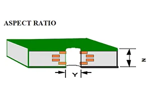
PCB aspect ratio refers to the ratio between the board thickness and the diameter of the smallest drilled hole, typically a via hole. This measurement, expressed as board thickness divided by via hole diameter, directly impacts the quality of electroplating during manufacturing. Poor aspect ratios lead to plating defects like voids or thin copper walls, which compromise electrical connectivity and mechanical strength. For electronic hobbyists, keeping this ratio in check prevents failures in multilayer boards or those with fine-pitch components. Industry standards such as IPC-2221 emphasize its role in reliable hole plating. Ultimately, a well-managed aspect ratio supports cost-effective production and long-term board performance.

High aspect ratios challenge the plating process because chemistry struggles to reach the hole's bottom uniformly. This can result in unreliable vias that fail under thermal stress or vibration, common in hobby projects like drones or wearables. Conversely, lower ratios promote even copper deposition, enhancing signal integrity and solderability. Hobbyists often overlook this until prototypes return with defects, delaying projects. Calculating PCB aspect ratio early in design saves time and resources. Awareness of board thickness and via hole diameter interplay empowers better decisions.
The Technical Principles Behind PCB Aspect Ratio
The core principle stems from the physics of electroplating in narrow, deep holes. When a via is drilled, its walls must receive a uniform copper layer for conductivity. Board thickness represents the hole depth, while via hole diameter sets the width, creating the aspect ratio. Higher ratios mean longer paths for plating ions, increasing defect risks. Materials like FR-4 influence drill quality, but the ratio remains the key metric. Standards like IPC-6012 outline performance criteria tied to these dimensions.
Drilling creates a rough hole that plating smooths, but excessive depth relative to diameter causes uneven buildup. Acidic or alkaline plating baths have limits on throw power, the ability to plate deep structures. Hobbyists using standard 1.6 mm boards must select via sizes accordingly to stay within practical limits. Aspect ratio also affects aspect ratio calculation example scenarios, where small changes in via hole diameter yield big reliability gains. Understanding these mechanisms allows informed trade-offs between density and manufacturability. This knowledge aligns hobby designs with professional practices.
Factors Influencing PCB Aspect Ratio
Several elements determine feasible aspect ratios in your designs. Board thickness, often standardized at 1.6 mm for single or double-layer boards, sets the numerator in the formula. Via hole diameter, chosen based on routing needs and component leads, forms the denominator. Multilayer boards increase thickness, demanding larger vias or advanced techniques. Plating chemistry and fab capabilities further constrain options, though hobby services handle common ratios well.
Via type matters too: through-hole vias span full thickness, while blind or buried ones reduce effective depth. For hobbyists, sticking to through-hole simplifies calculations. IPC-A-600 provides acceptability criteria for plated holes influenced by aspect ratio. Environmental factors like humidity during fab can exacerbate issues in high-ratio boards. Balancing these ensures your project progresses smoothly. Always verify with your fab's guidelines alongside standard calculations.
How to Calculate PCB Aspect Ratio: Step-by-Step Guide
Calculating PCB aspect ratio starts with gathering precise measurements. First, determine your board thickness from the stack-up, including copper layers and prepreg. This value, in millimeters or mils, is the hole depth for through-vias. Next, identify the smallest via hole diameter specified in your design file, typically the drill size before plating shrinkage. Use consistent units to avoid errors.
The PCB aspect ratio formula is straightforward: divide board thickness by via hole diameter. For instance, a 1.6 mm thick board with a 0.3 mm via hole diameter yields 1.6 / 0.3 = 5.33, or about 5:1. Express it as a ratio like 5:1 for clarity. Repeat for all via sizes, focusing on the highest ratio which governs manufacturability. Tools like spreadsheets simplify iterations during design.
Step 1: Note board thickness T. Step 2: List smallest drill diameter D. Step 3: Compute AR = T / D. Step 4: Check against guidelines. Step 5: Adjust via sizes if needed. This process integrates easily into your workflow.
Practical Best Practices for Aspect Ratio Management
Aim for conservative ratios to ensure first-pass success in hobby projects. Select via hole diameters at least 0.25 mm for standard thicknesses, adjusting upward for multilayers. Use larger vias where possible to lower the ratio without sacrificing space. Incorporate via tents or fills for non-critical signals to reduce plating demands. Consult fab DFM reports post-calculation for confirmation.
Incorporate aspect ratio early by setting design rule checks in your software. For dense boards, consider blind vias to cut effective depth, though they raise costs. Maintain drill-to-copper clearances per standards. Test prototypes with continuity checks on high-ratio vias. These habits build reliable hobby electronics. Regular reviews prevent recurring issues.
Aspect Ratio Calculation Example for Real-World Application
Consider a double-layer hobby board at 1.6 mm thick with power and signal vias. The smallest via needs a 0.2 mm drill for tight routing. Applying the PCB aspect ratio formula: 1.6 / 0.2 = 8, or 8:1. This common setup works for many fabs but borders on challenging for plating.
If routing allows, enlarge to 0.25 mm: 1.6 / 0.25 = 6.4:1, improving reliability. For a thicker 2.4 mm four-layer board, 0.3 mm vias give 2.4 / 0.3 = 8:1 again. Experimenting with examples reveals trade-offs. Document ratios in your design notes. Such calculations guide iterative improvements.
Common Pitfalls and Troubleshooting Tips
Overlooking the smallest via leads to surprises during fab quotes. Always scan Gerbers for min drill size. High ratios cause barrel cracks under thermal cycling, fixable by redesigning. Uneven plating shows as high resistance; inspect with a multimeter. If issues arise, downsize board thickness or upscale vias.
Software defaults may permit risky ratios, so override with custom rules. Humidity warps thin boards, worsening high-ratio holes. Bake boards pre-assembly if needed. Learning from failures refines skills. Persistent problems warrant fab consultation.
Conclusion
Mastering PCB aspect ratio equips electronic hobbyists for successful designs. The simple formula of board thickness over via hole diameter unlocks reliable manufacturing. Follow the steps to calculate PCB aspect ratio routinely, using examples to validate choices. Adhere to principles from standards like IPC-2221 and IPC-6012 for quality. With practice, you'll produce durable boards that power innovative projects. Start applying these insights today for frustration-free prototyping.
FAQs
Q1: What is the PCB aspect ratio formula?
A1: The PCB aspect ratio formula is board thickness divided by the smallest via hole diameter. This yields a ratio like 6:1, guiding plating feasibility. Use it early to balance density and reliability. Hobbyists benefit from quick spreadsheet checks. Standards reference it for design validation.
Q2: How do I calculate PCB aspect ratio for a beginner project?
A2: Measure board thickness from your stack-up, note the smallest drill diameter, then divide thickness by diameter. For a 1.6 mm board and 0.3 mm via, it's about 5:1. Verify all vias for the worst case. Adjust for multilayers. This ensures smooth fab handover.
Q3: Why is via hole diameter critical in aspect ratio calculation example?
A3: Via hole diameter sets the denominator, directly lowering the ratio when increased. In examples, upsizing from 0.2 mm to 0.3 mm on a 1.6 mm board drops from 8:1 to 5:1, easing plating. Smaller diameters suit density but risk defects. Balance with routing needs.
Q4: What role does board thickness play in calculate PCB aspect ratio?
A4: Board thickness is the hole depth, raising the ratio as it grows. Standard 1.6 mm suits hobby boards, but thicker multilayers demand larger vias. Control it via layer count. Pair with diameter for optimal results. This prevents common plating failures.
References
IPC-2221B — Generic Standard on Printed Board Design. IPC, 2012
IPC-6012F — Qualification and Performance Specification for Rigid Printed Boards. IPC, 2023
IPC-A-600K — Acceptability of Printed Boards. IPC, 2020


